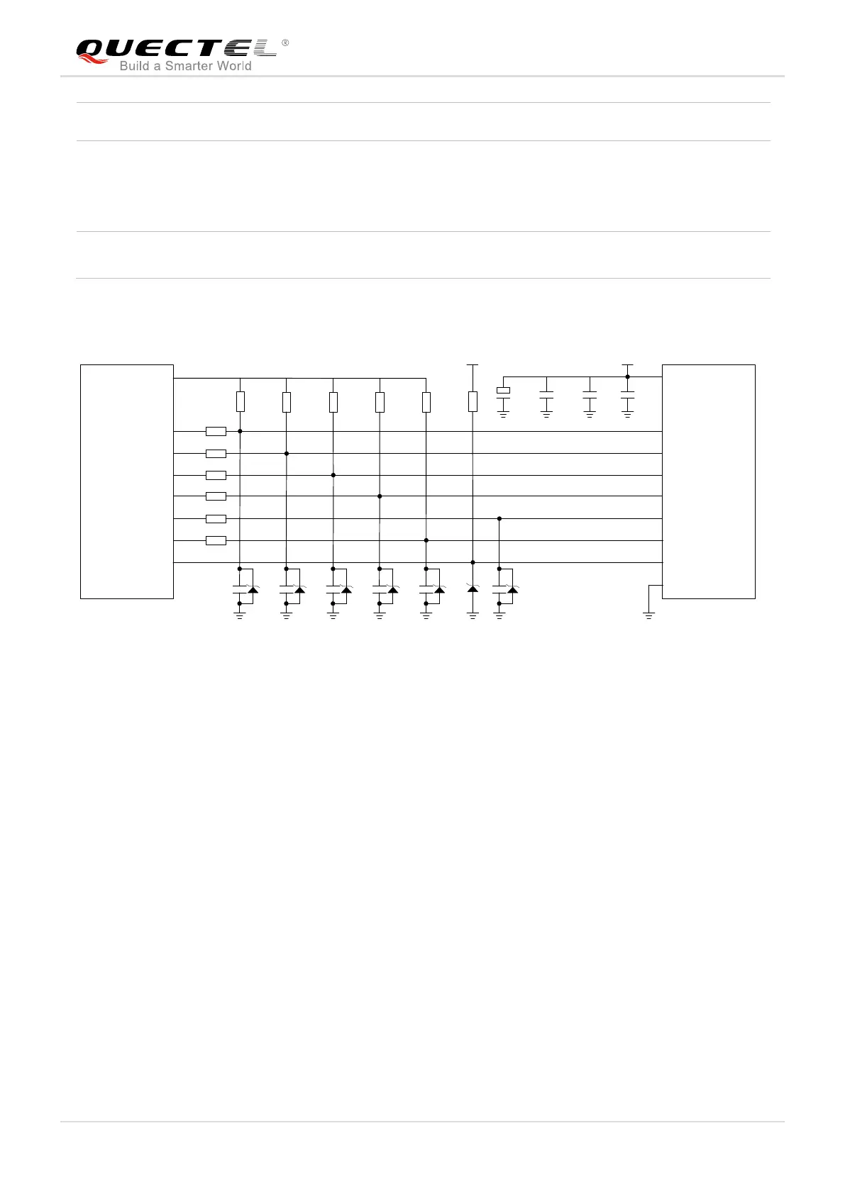
Figure 25: Reference Circuit of SD Card
In SD card interface design, in order to ensure good communication performance with SD card, the
following design principles should be complied with:
SD_INS_DET must be connected.
The voltage range of SD card power supply VDD_3V is 2.7V~3.6V and a sufficient current up to 0.8A
should be provided. As the maximum output current of VDD_SDIO is 50mA which can only be used
for SDIO pull-up resistors, an externally power supply is needed for SD card.
To avoid jitter of bus, resistors R7~R11 are needed to pull up the SDIO to VDD_SDIO. Value of these
resistors is among 10KΩ~100KΩ and the recommended value is 100KΩ. VDD_SDIO should be used
as the pull-up power.
In order to adjust signal quality, it is recommended to add 0Ω resistors R1~R6 in series between the
module and the SD card. The bypass capacitors C1~C6 are reserved and not mounted by default. All
resistors and bypass capacitors should be placed close to the module.
In order to offer good ESD protection, it is recommended to add a TVS diode on SD card pins near
the SD card connector with junction capacitance less than 15pF.
Keep SDIO signals far away from other sensitive circuits/signals such as RF circuits, analog signals,
etc., as well as noisy signals such as clock signals, DCDC signals, etc.

 Loading...


