Programming Information
105
Doc No: UMAN\FL\0110
Rev. No.: 1.02B
7.2 Memory Allocation of XW, YW and MW
Memory for XW, YW and MW registers for particular model is allocated by software at the time of I/O allocation. The
number of XW, YW and MW for the particular model is as per the table given below:
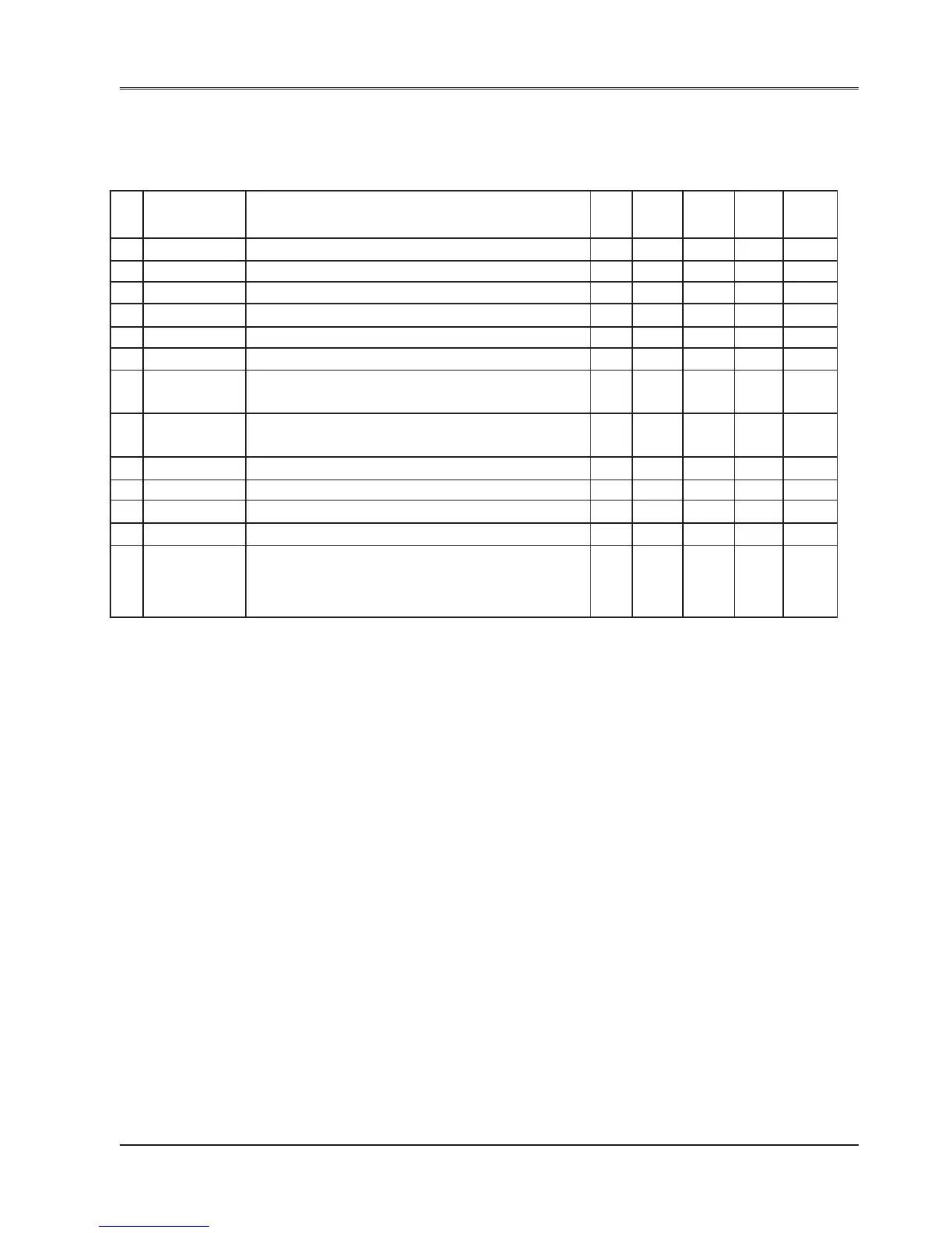
Sr. Model Name Description XW YW MW X Y
No.
1 FL010 FlexiLogics Base Model 1 1 60 8 8
2 FL050 FlexiLogics Base Module with Ethernet 0 0 60 0 0
3 FLD1600 16 Input Digital Module 100160
4 FLD0016P 16 PNP type transistor output digital module 010016
5 FLD0016N 16 NPN type transistor output digital module 010016
6 FLD0016R 16 Relay type output digital module 010016
7 FLD0808P 8 Digital input, 8 PNP type transistor output digital 11088
module
8 FLD0808N 8 Digital input, 8 NPN type transistor output digital 11088
module
9 FLD0808R 8 Digital input, 8 Relay type output digital module 11088
10 FLA0800L 0-10 VDC or 4-20 mA (16 Bit) 8 channel input model 8 0 50 0 0
11 FLA0004 0-10 VDC or 4-20 mA (16 Bit) 4 channel output model 0 4 30 0 0
12 FLA0800R PT100 RTD (16 Bit) 8 channel input model 8 0 50 0 0
13 FLA0402U 4 Universal Analog Inputs ( RTD, TC, 4-20 mA, 4 2 40 0 0
0-20mA,0-50mV, 0-100mV, 0-10VDC) (16 Bit),
2 channel Voltage/Current (16 Bit) outputs.
The allocation is sequential. If any particular model does not have XW / YW / MW defined then the memory is not
allocated in the array for that model. This array is sequentially mapped to Modbus registers.
Consider the example that user has configured the models as below:
Slot 0 : FL010 : XW : 1, YW : 1, MW : 60
Slot 1 : FLD0808R : XW : 1, YW : 1, MW : 0
Slot 2 : FLD0016R : XW : 0, YW : 1, MW : 0
Slot 3 : FLD0808N : XW : 1, YW : 1, MW : 0
Slot 4 : FLD1600 : XW : 1, YW : 0, MW : 0
Slot 5 : FLA0800L : XW : 8, YW : 0, MW : 50