This section details the physical specifications
of
the host/drive interface con-
nectors. Connector dimensions
and
pin assignments
foHow
under each section.
Refer below
to
Figure 7 for an overall view
of
the drive interface connectors.
2.1
CONTROL AND STATUS SIGNALS:
PCB EDGE-CONNECTOR
J1
2.0
ST212
HOST/DRIVE
INTERFACE
Do
not
touch the
peB
edge-connectors, board components
or
the printed cir·
cuit cable without observing static-discharge precautions. Handle the drive
by
the frame only.
Control
and
status signais between the host and the drive are transmitted through
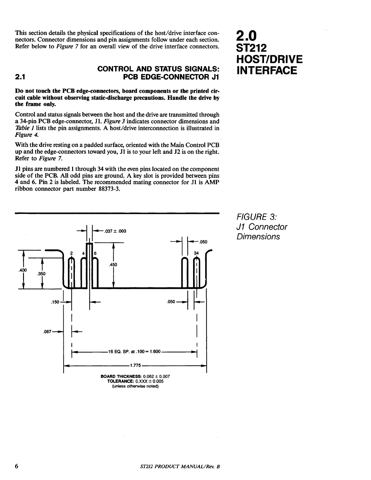
a 34-pin PCB edge-connector,
JI.
Figure 3 indicates connector dimensions
and
Table
llists
the pin assignments. A host/drive interconnection
is
illustrated in
Figure
4.
Withthe drive resting
on
a padded surface, oriented with the Main Control PCB
up
and
the edge-connectors toward you,
11
is
to your left
and
J2
is on the right.
Refer to
Figure
7.
JI
pins are numbered 1through 34 with the even pins located
on
the component
side
of
the PCB.
AH
odd
pins are ground. A
key
slot is provided between pins
4
and
6.
Pin 2 is labeled. The recommended mating connector for
11
is
AMP
ribbon connector
part
number 88373-3.
6
.087
-l
r
.037
±.003
~
.450
1
~
1 1
1-
..
----16
EQ.
SP.
at
.100=
1.600-----II
..
~1
1-.--------1.775--------.-j
BOARD THICKNESS: 0.062 ± 0.007
TOLERANCE:
O.XXX
± 0.005
(unless otherwise noted)
ST212 PRODUCT
MANUAL/Rev.
B
FIGURE
3:
J1
Connector
Dimensions