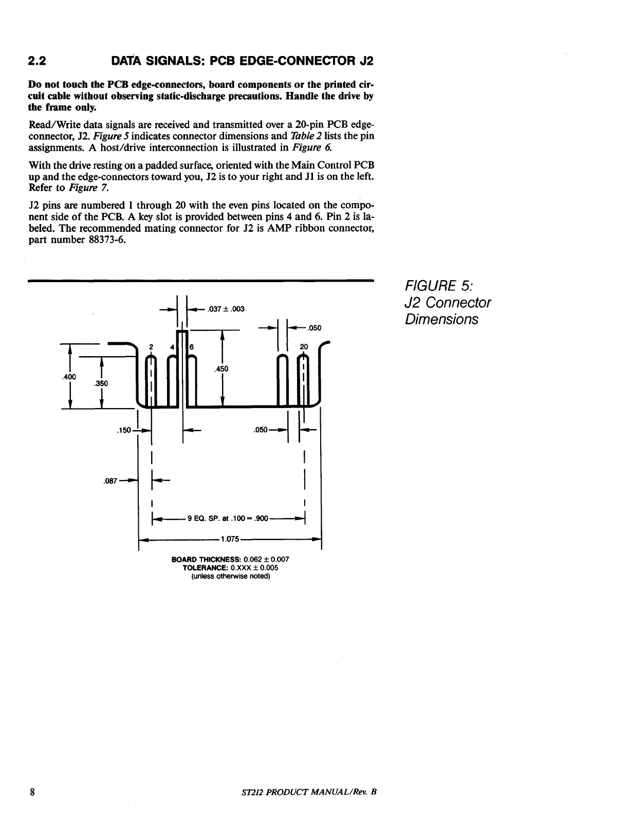
2.2
DATA
SIGNALS: PCB EDGE-CONNECTOR
J2
Do
not
touch the
PCB
edge.connectors, board components
or
the printed cir-
cuit cable without observing static-discharge precautions. Handle the drive by
the frame ooly.
Read/Write
data
signaIs are received
and
transmitted over a 20-pin PCB edge-
connector, J2.
Figure 5 indicates connector dimensions
and
Table
2lists
the pin
assignments. A host/drive interconnection
is
illustrated in Figure
6.
With thedrive resting
on
a padded surface, oriented with the Main Control PCB
up
and
the edge-connectors toward you,
J2
is
to your right
and
JI
is
on
the left.
Refer
to
Figure
7.
J2
pins are numbered 1 through 20 with the even pins located
on
the compo-
nent side
of
the PCB. A
key
slot
is
provided between pins 4
and
6. Pin 2 is la-
beled. The recommended mating connector for J2
is
AMP
ribbon connector,
part
number 88373-6.
FIGURE 5:
J2
Connector
Dimensions
1--.
050
1 20
ooo~
~
1
1
.450
2 4
1
.087
~
Fr------I
.400
LL""I+I-
....
"
....
------
...........
~
.150 1
1
1-
1
9 EO. SP. at .100 =
.900---1
__
1
.-------1.075-------I~
BOARD
THICKNESS: 0.062 ± 0.007
TOLERANCE:
O.XXX
± 0.005
(unless otherwise noted)
8
ST212
PRODUCT MANUAL/Rev. B