6.6.5 Wiring digital switching outputs
Physical switching outputs on the device
The physical switching outputs can be allocated independently of each other with vari‐
ous functions for event status indication. If the allocated event occurs in the read proc‐
ess, then the corresponding switching output is live after the end of the clock reading
pulse for the selected pulse duration.
Depending on the device, there are different numbers of switching outputs available on
the connections, see "Pin allocation of the connections", page 36.
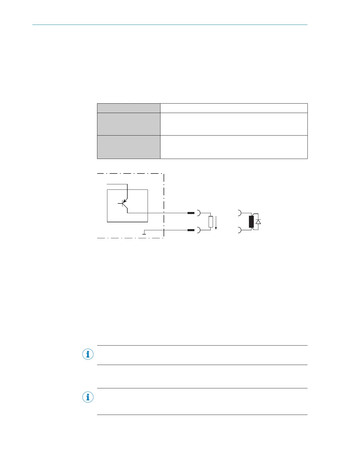
Switching behavior PNP switching to supply voltage V
S
Properties Short-circuit protected
Temperature protected
Not electrically isolated from V
S
Electrical values The electrical values are identical for all switching outputs.
0 V ≤ V
out
≤ V
S
(V
S
−1.5 V) ≤ V
out
≤ V
S
at I
out
≤ 100 mA
V
out
3
4
Switching output 1
!
"
Signal 2
GND
Figure 42: Wiring of a switching output
1
Switching output (“Result 1” or “Result 2”)
2
Output signal
3
Output voltage V
out
4
With an inductive load: Sweep-out circuit – attach a freewheeling diode directly to the
load.
!..."
For pin assignment, see respective device
Extension: additional logical switching outputs in the device in the case of physical
“external” switching outputs on the optional connection module
Thanks to the optional CMC600 parameter memory module, the two additional switch‐
ing outputs “External output 1” and “External output 2” on the terminals in the connec‐
tion module are additionally available.
NOTE
These two external switching outputs are not suitable for time-critical applications.
If the wiring of the outputs is carried out via a connection module, then the relevant
operating instructions for the module must be followed.
NOTE
Capacitive loads on the switching outputs have an effect on the switch-on and switch-
off behavior. The maximum capacity of 100 nF is a limit value.
ELECTRICAL INSTALLATION 6
8014396/ZMG8/2017-07-04 | SICK O P E R A T I N G I N S T R U C T I O N S | CLV69x
49
Subject to change without notice