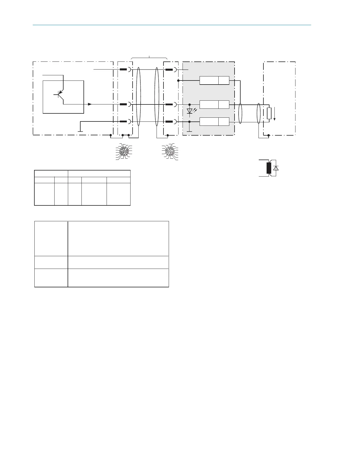
Wire switching outputs “Result 1 ... 4” of the CLV69x in the CDB650-204 connection module
CLV69x
CDB650-204
Load (e.g. PLC)
Y
1
.
.
.
Z
Name
22
GND
5Shield
U
IN
*U
V
GND
U
a
Result X
GND
Y
1
2
2)
2
Discharge wiring:
apply free running
diode directly to
the load!
In the case of inductive load:
17
16
10
11
12
15
14
6
5
4
13
7
8
9
1
2
3
17
16
10
11
12
15
14
6
5
4
13
7
8
9
1
2
3
M12,
17-pin,
A-coded
CDB650-204CLV69x
Terminal ZNamePin YPin YResult X
20
21
50
51
RES/OUT 1
RES/OUT 2
RES/OUT 3
RES/OUT 4
13
14
16
17
13
14
16
17
Result 1
Result 2
Result 3
Result 4
For CLV69x-xxx0 (without heating):
no. 6052286 (2m)
no. 6051194 (3m)
no. 6051195 (5m)
For CLV69x-xxx1 (with heating):
no. 6053230 (2m)
no. 6053231 (3m)
no. 6053232 (5m)
2) Pin 2 in the CLV69x-xxx1
(with heating) not connected
1) Dependent on type
Specifications of the switching outputs “Result 1 ... 4”
Functional allocation for switching outputs via SOPAS-ET
configuration software.
Connection cable 1:1
1)
Logic
Properties
Electrical
values
PNP switching to supply voltage U
V
.
CLV69x default:
Result 1: Device Ready (static), logic: active high
Result 2: Good Read, 100mm, logic: active high
Result 3: no function assigned
Result 4: no function assigned
– Short-circuit protected + temperature protected
– Not electrically isolated from U
V
(+ 24V*)
0V ≤ U
a
≤ U
V
Guaranteed:
(U
V
− 1.6V) ≤ U
a
≤ U
V
in the case of I
a
≤ 100mA