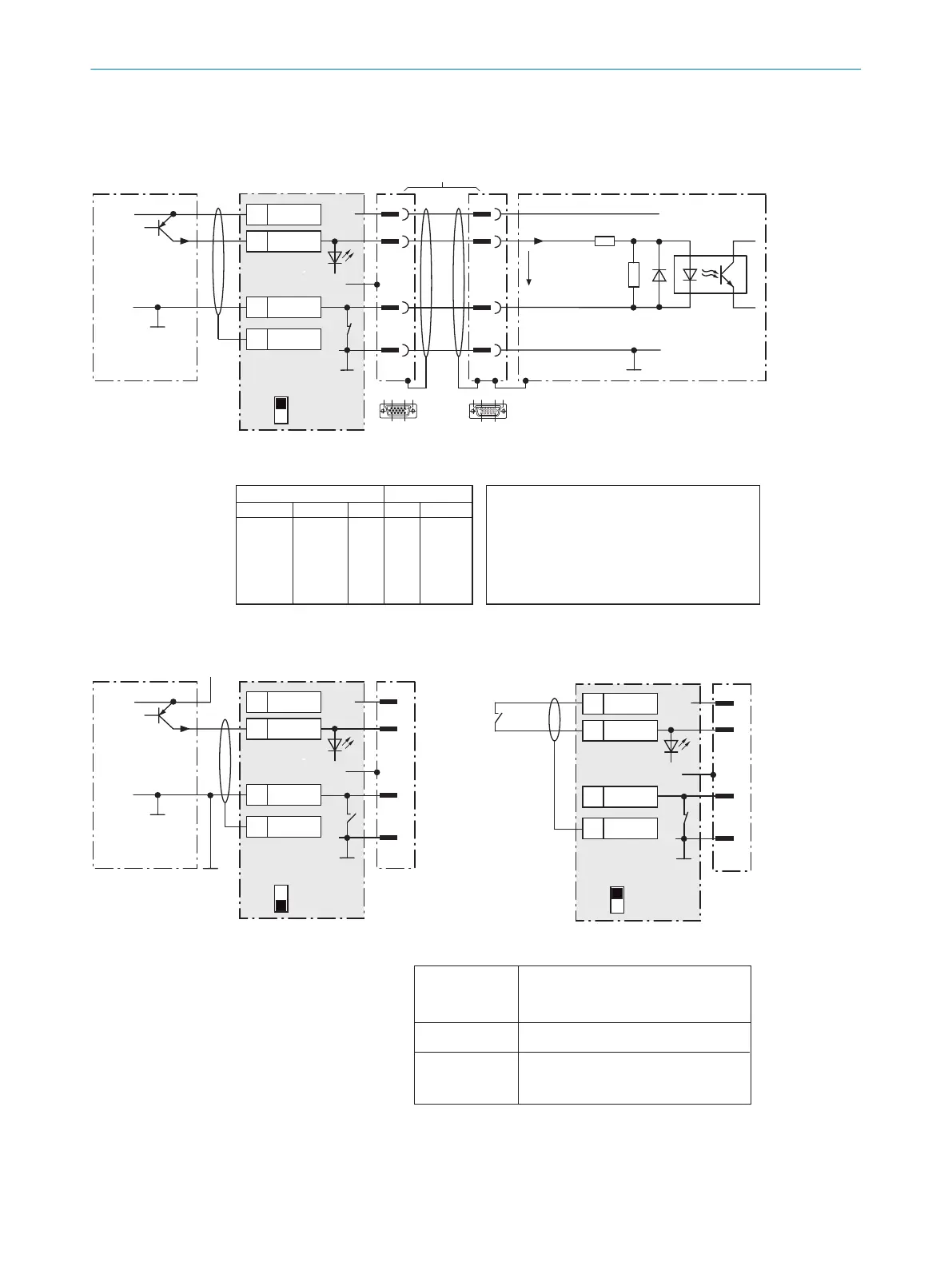
Wire “Sensor 1 ... 6” switching inputs of the CLV69x in the CDM490-0001 connection module
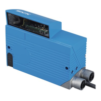
CLV69x
PNP sensor
U
V
U
V
U
V
GND
GND
SensGND
3,32K
6,64K
Sensor Z
U
e
9
a) Schema: sensor supplied by CDM490-0001
b) Schema: sensor connected volt-free and externally supplied
d) Schema: switch connected volt-free
and externally supplied
1
Y
9
Y
5
1
5
Out
+24V*
+24V*
GND
S1
e.g. photoelectric sensor
PNP sensor
U
V
GND
Connection of the switch as under b)
Out
GND
S1
e.g. photoelectric
sensor
ON
OFF
S1 : SGND
ON
OFF
S1 : SGND
U
V ext
Characteristic data of the switching inputs “Sensor 1 ... 6”
Current at the input starts the
assigned function, e.g. start reading cycle.
(CLV69x default settings:
logic active high, debouncing 10mm)
– Opto-decoupled, reverse-polarity protected
– Can be wired with PNP output of a sensor
Low: U
e
≤ 2V; I
e
≤ 0,3mA
High: 6V ≤ U
e
≤ 32V;
0,7mA ≤ I
e
≤ 5mA
Switching behavior
Properties
Electrical values
Switch S1: SGND
ON: connect GND of the switching inputs to the
GND of the CDM490-0001/CLV69x.
OFF: sensors connected volt-free to switching inputs
on the CDM490-0001/CLV69x.
Reference potential valid for all “Sensor 1 ... 6”
switching inputs and optionally
Shield
1) E.g. no. 2020302 (3m)
GND
.
.
.
Shield
X
Name
54
SGND
6
Shield
51
+24V*
X
Name
54
SGND
6
Shield
51
+24V*
U
e
= max. 32V
a) Schema: switch supplied by CDM490-0001
+24V*
GND
S1
ON
OFF
S1 : SGND
Shield
X
Name
54
SGND
6
Shield
51
+24V*
2 “I/O” connection
2
6
1
10
5
11
15
10 5 61
15 11
15-pin
D-Sub-HD
male connector
15-pin
D-Sub-HD
female connector
CDM490-0001 CLV69x
Terminal X
61
62
63
64
65
66
Name
Sensor
IN 0
IN 1
IN 2
IN 3
IN 4
Pin Y
3
6
2
7
11
12
Pin Y
3
6
2
7
11
12
Sensor Z
Sensor 1
Sensor 2
Sensor 3
Sensor 4
Sensor 5
Sensor 6
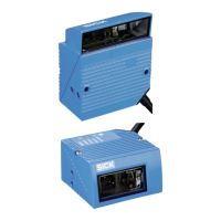
CDM490-0001
(I/O card)
CDM490-0001
(I/O card)
CDM490-0001
(I/O card)
Adapter cable
1)