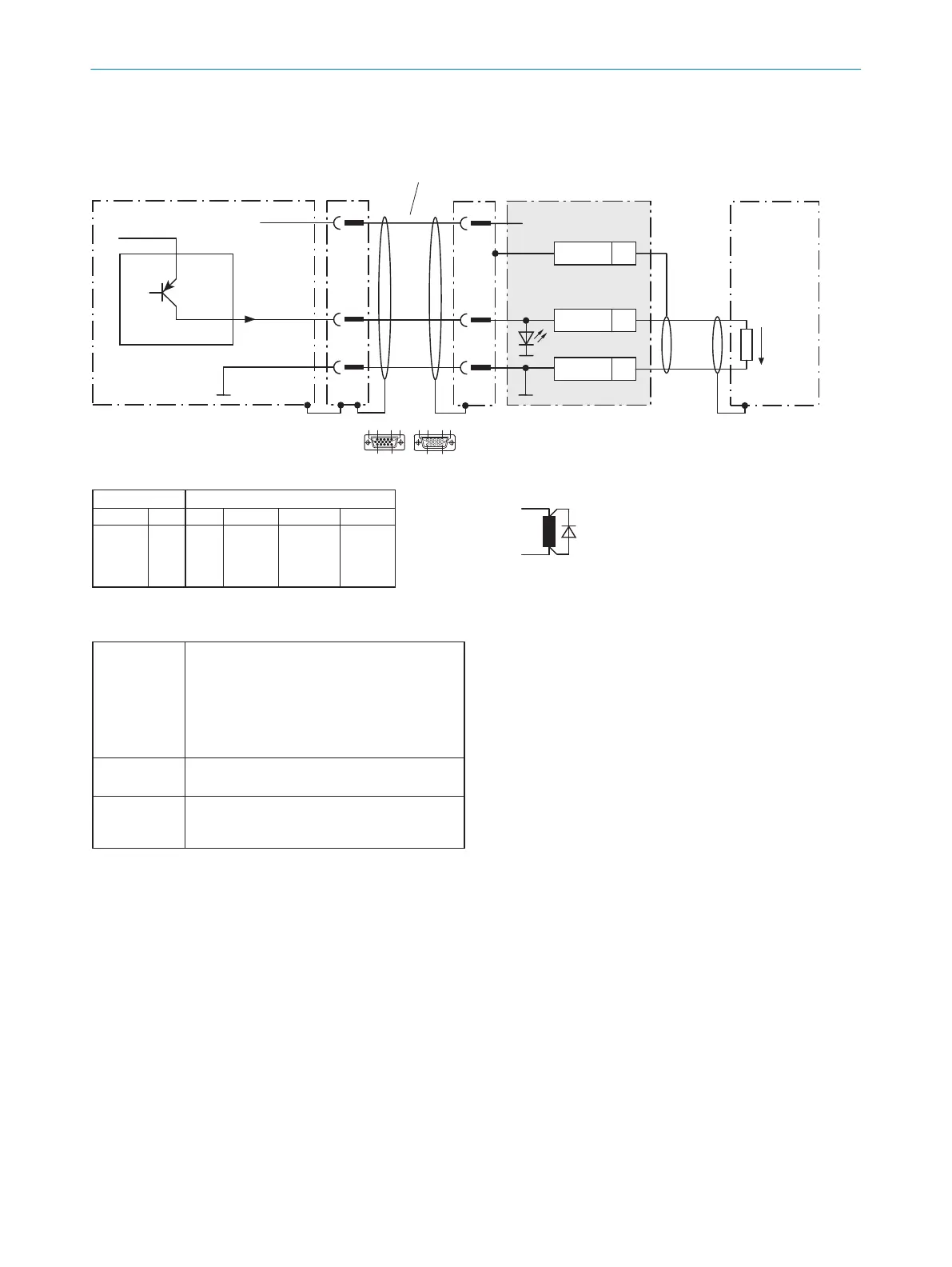
Wire “Result 1 ... 4” switching outputs of the CLV69x in the CDM490-0001 connection module
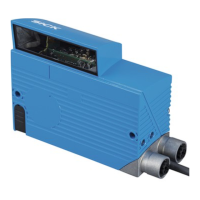
CLV69x
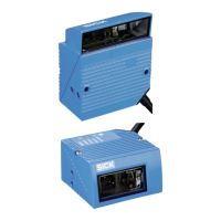
CDM490-0001
(I/O card)
U
V
= DC 18 ... 30V
Load (e.g. PLC)
Cable, e.g.
No. 2020302 (3m)
Y
5
.
.
.
Z
Name
45
GND
5
Shield
+24V* (U
V
)
U
V
GND
Sweep-out circuit:
Attach a freewheeling diode
directly to the load.
With inductive load:
U
a
Result X
Result X
GND
Y
5
1 1
Characteristic data of “Result 1 ... 4“ switching outputs
PNP switching to supply voltage
U
V
(+24V*).
CLV69x default settings:
Result 1: device ready (static), logic: active high
Result 2: good read, 100mm, logic: active high
Result 3: no function assigned
Result 4: no function assigned
– Short-circuit protected + temperature protected
– Not electrically isolated from U
V
(+24V*)
0V ≤ U
a
≤ U
V
Guaranteed:
(U
V
− 1.6V) ≤ U
a
≤ U
V
at I
a
≤ 100mA
Switching
behavior
Properties
Electrical
values
2 “I/O” connection
2
6
1
10
5
11
15
10 5 61
15 11
D-Sub-HD
CDM490-0001CLV69x
Terminal Z
41
42
43
44
Name
Result 1
Result 2
Result 3
Result 4
Pin Y
4
8
10
15
Pin Y
4
8
10
15
Result X
Result 1
Result 2
Result 3
Result 4
Result X
Result 1
Result 2
Result 3
Result 4