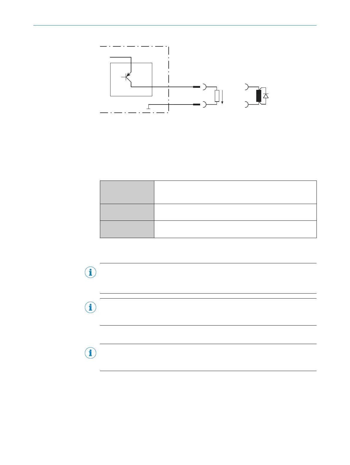
V
out
3
4
Switching output of device 1
!
"
Signal 2
GND
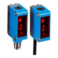
Figure 21: Wiring a digital output
1
Digital output of the device (“Result 1” to “Result 3”)
2
Output signal
3
Output voltage V
out
4
With inductive load: see note
!... "
For pin assignment, see respective device
Table 12: Characteristic data of the digital outputs
Switching behavior PNP switching to supply voltage V
S
Default: No function
Logic: not inverted (active high)
Properties
•
Short-circuit protected
•
Not electrically isolated from V
S
1)
Electrical values 0 V ≤ V
out
2)
≤ V
S
(V
S
−1.5 V) ≤ V
out
≤ V
S
at I
out
3)
≤ 50 mA
1)
Supply voltage.
2)
Output voltage.
3)
Output current.
NOTE
Provide an arc-suppression switch at the digital output if inductive load is present.
b
Attach a freewheeling diode directly to the load for this purpose.
NOTE
Capacitive loads on the digital outputs have an effect on the switch-on and switch-off
behavior. A maximum capacitance of 100 nF is the limit value.
Function assignment
NOTE
Assign the functions for the digital outputs in the device using a configuration tool, e.g.
the configuration software SOPAS ET.
6 ELECTRICAL INSTALLATION
38
O P E R A T I N G I N S T R U C T I O N S | GLS611 8026021//2020-12-18 | SICK
Subject to change without notice