Signal 3
52.3 K
3 K
"
§
$
Sensor GND
V
S
2
V
S
V
S
V
in
5
!
PNP sensor 1
GND
GND
Switching input of device 4
GND
V
S
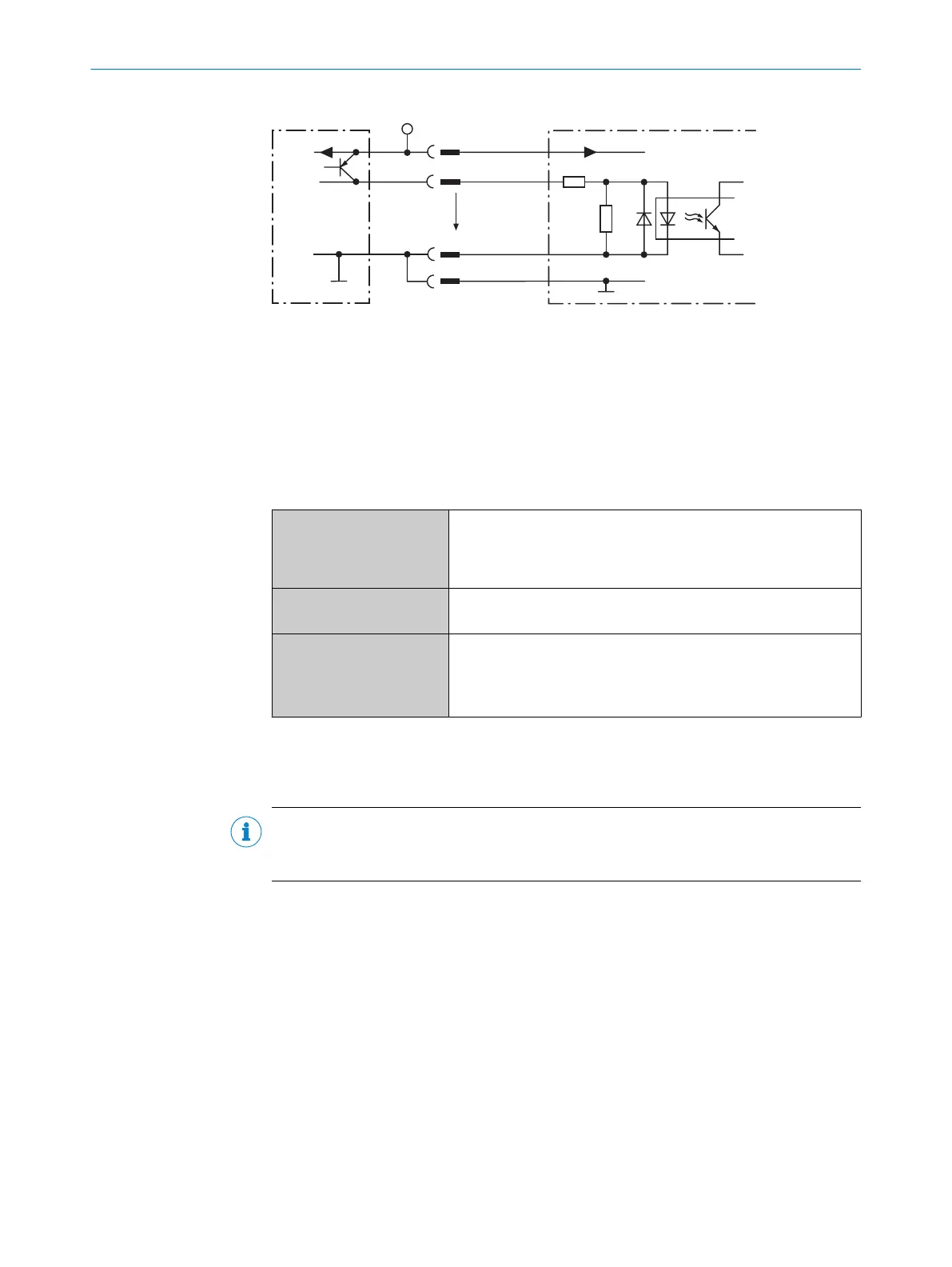
Figure 20: Wiring a digital input
1
Trigger sensor (PNP sensor)
2
Supply voltage V
S
3
Input signal
4
Digital input of the device (“Sensor 1” or “Sensor 2”)
5
Input voltage V
in
!... $
For pin assignment, see respective device
Table 11: Characteristic data of the digital inputs “Sensor 1” and “Sensor 2”
Switching behavior Signal on the input starts the assigned function, e.g. start of the
internal reading interval of the device.
Default: active high
Debouncing: 10 ms (standard)
Properties
•
Opto-decoupled, reverse polarity protected
•
Can be wired with PNP output of a trigger sensor
Electrical values The electrical values are identical for all digital inputs of the
device.
Low: V
in
1)
≤ 2 V; I
in
2)
≤ 0.3 mA
High: 6 V ≤ V
in
≤ 27.6 V; 0.7 mA ≤ I
in
≤ 5 mA
1)
Input voltage.
2)
Input current.
Function assignment
NOTE
Assign the functions for the digital inputs in the device using a configuration tool, e.g.
the configuration software SOPAS ET.
6.5.5 Wiring the digital outputs
The “Result 1” to “Result 3” digital outputs are used to signal events in the read opera‐
tion. Different functions can be assigned to them independently of each other for this
purpose. If the assigned event occurs, then the corresponding digital output becomes
live after the end of the read cycle for the selected pulse duration, for example (default).
The full complement of digital outputs is available at each of the following locations:
•
Male connector of the device cable (M12, 17-pin, A-coded)
•
Open end of the adapter cable (female connector, M12, 17-pin, A-coded/open
end)
ELECTRICAL INSTALLATION 6
8026021//2020-12-18 | SICK O P E R A T I N G I N S T R U C T I O N S | GLS611
37
Subject to change without notice