Hardware Information
Release 04/02
7-34
Panel PC 670 Computing Unit, Equipment Manual
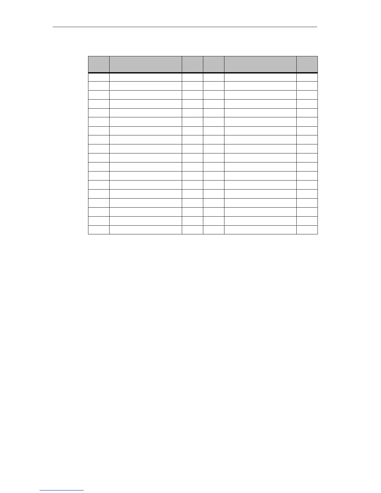
Pin Signal Name Type
*
Pin Signal Name Type
C1 –SBHE O D1 –MEMCS16 I
C2 LA 23 I/O D2 –IOCS16 I
C3 LA 22 I/O D3 IRQ 10 I
C4 LA 21 I/O D4 IRQ 11 I
C5 LA 20 I/O D5 IRQ 12 I
C6 LA 19 I/O D6 IRQ 13 I
C7 LA 18 I/O D7 IRQ 14 I
C8 LA 17 I/O D8 –DACK0 O
C9 –MEMR I/O D9 DRQ 0 I
C10 –MEMW I/O D10 –DACK5 O
C11 SD 08 I/O D11 DRQ 5 I
C12 SD 09 I/O D12 –DACK6 O
C13 SD 10 I/O D13 DRQ 6 I
C14 SD 11 I/O D14 –DACK7 O
C15 SD 12 I/O D15 DRQ 7 I
C16 SD 13 I/O D16 + 5V V
CC
C17 SD 14 I/O D17 –MASTER I
C18 SD 15 I/O D18 0 V GND
Under normal conditions, the signals –SBHE, LA17 – LA23, –MEMR and MEMW
are operated as outputs (sending from CPU). Only CPU modules that are suitable
for use as a master CPU for system bus access send and receive these signals. A
minus sign, ”–”, in front of the signal name shows that the signal is LOW active.
7.6.3 Pin assignment PCI slot
The table on the next page resumes the pin assignment of the PCI slot.