Pin Signal name Type Pin Signal name Type
25 DI117.3 26 DO117.3
27 DI117.4 28 DO117.4
29 DI117.5 30 DO117.5
31 DI117.6 32 DO117.6
33 DI117.7 34 DO117.7
35 DI121.0 36 DI121.1 I
37 DI121.2 38 DI121.3 I
39 Reserved 40 Reserved
Table 7-50 Assignment of connector X114
Pin Signal name Type Pin Signal name Type
1 Ground V 2 Ground V
3 DI118.0 I 4 DO118.0 O
5 DI118.1 6 DO118.1
7 DI118.2 8 DO118.2
9 DI118.3 10 DO118.3
11 DI118.4 12 DO118.4
13 DI118.5 14 DO118.5
15 DI118.6 16 DO118.6
17 DI118.7 18 DO118.7
19 DI119.0 20 DO119.0
21 DI119.1 22 DO119.1
23 DI119.2 24 DO119.2
25 DI119.3 26 DO119.3
27 DI119.4 28 DO119.4
29 DI119.5 30 DO119.5
31 DI119.6 32 DO119.6
33 DI119.7 34 DO119.7
35 DI121.4 36 DI121.5 I
37 DI121.6 38 DI121.7 I
39 Reserved 40 Reserved
Table 7-51 Technical data of the inputs of X111 to X114
Parameter Value
Voltage: 0 V to 5 V
Typical current consumption: 0.2 mA at 5 VDC
-0.3 mA at 0 VDC
Signal level (including ripple): High signal level: 2.3 V to 5 V
Low signal level: 0 V to 1 V
Connectable components
7.3 MCP Interface PN
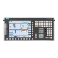
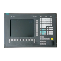
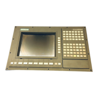
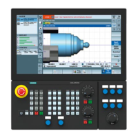
PPU
144 Manual, 01/2014, 6FC5397-2DP40-3BA3
 Loading...