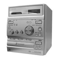
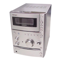
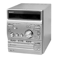
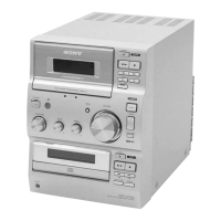
TUNER board
POWER board
AUDIO board
LEAF SWITCH board
LCD board
CONTROL board
Note on Printed Wiring Board:
• X : parts extracted from the component side.
• Y : parts extracted from the conductor side.
• x : parts mounted on the conductor side.
• b : Pattern from the side which enables seeing.
(The other layers' patterns are not indicated.)
Note on Schematic Diagram:
• All capacitors are in µF unless otherwise noted. pF: µµF
50 WV or less are not indicated except for electrolytics
and tantalums.
• All resistors are in Ω and
1
/
4
W or less unless otherwise
specified.
• 5 : fusible resistor.
• U : B+ Line.
• V : B– Line.
• H : adjustment for repair.
• Voltages are taken with a VOM (Input impedance 10 MΩ).
Voltage variations may be noted due to normal produc-
tion tolerances.
• Waveforms are taken with a oscilloscope.
Voltage variations may be noted due to normal produc-
tion tolerances.
• Circled numbers refer to waveforms.
• Signal path.
F : TUNER (FM/AM)
E : PLAYBACK (DECK A)
d : PLAYBACK (DECK B)
a :RECORD
J : CD PLAY (ANALOG OUT)
c : CD PLAY (DIGITAL OUT)
• Abbreviation
AUS : Australian model
AED : North European model
EA : Saudi Arabia model
SP : Singapore model
Note: The components identified by mark 0 or dotted line
with mark 0 are critical for safety.
Replace only with part number specified.