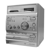
44
7-21. IC PIN FUNCTION DESCRIPTION
• MAIN BOARD IC802 CXP84332-168Q (SYSTEM CONTROLLER)
Pin No. Pin Name I/O Description
1 A/B O Deck-A/B selection signal output to the HA12203NT (IC401) “L”: deck-A, “H”: deck-B
2 AMP-STBY O Standby on/off control signal output to the power amplifier (IC101, 201) “L”: standby mode
3 HI DUB REC O High speed dubbing control signal output to the HA12203NT (IC401)
4 C-XRST O Reset signal output to the CXA1992BR (IC701) and CXD2589Q (IC703) “L”: reset
5 SPEAK RELAY O Speaker protect relay drive signal output terminal “H”: relay on
6 AMP-MUTE O Muting on/off control signal output to the power amplifier (IC101, 201) “H”: muting on
7 REC-BIAS O
Recording bias on/off selection signal output to the HA12203NT (IC401)
“L”: bias on, “H”: bias off
8 REC/PB O
Recording/playback/pass selection signal output to the HA12203NT (IC401)
“L”: recording mode, “H”: pass, “Hi-z”: playback mode
9
CAP MOTOR
CON
O Capstan motor on/off control signal output terminal “H”: motor on
10
CAP MOTOR
H/L
O
High/normal speed selection signal output of the capstan motor
“L”: normal speed, “H”: high speed
11
TRIG MOTOR
CON (A)
O
Deck-A side trigger motor drive signal output to the trigger motor drive (IC402)
“H”: motor on
12
TRIG MOTOR
CON (B)
O
Deck-B side trigger motor drive signal output to the trigger motor drive (IC402)
“H”: motor on
13
TRIG MOTOR
H/L
O Trigger motor control signal output terminal
14 T-HALF (A) I
Detection input from the deck-A cassette detect switch (S1003)
“L”: cassette in, “H”: no cassette
15 T-PLAY (A) I Detection input from the deck-A play detect switch (S1001) “H”: deck-A play
16 TC-SHUT (A) I Shut off detection signal input from the deck-A side reel pulse detector (Q1001)
17 TC-SHUT (B) I Shut off detection signal input from the deck-B side reel pulse detector (Q1002)
18 T-PLAY (B) I Detection input from the deck-B play detect switch (S1002) “H”: deck-B play
19 TU-TUNED I Tuning detection signal input from the tuner pack “L”: tuned
20 TU-DATA O PLL serial data output to the tuner pack
21 TU-CLK O PLL serial data transfer clock signal output to the tuner pack
22 TU-COUNT I PLL serial data input from the tuner pack
23 TU-CE O PLL chip enable signal output to the tuner pack
24 RDS-DATA I
RDS serial data input from the RDS decoder (IC803)
(Used for the AEP, UK and North European models only)
25 RDS-ON O
Power supply on/off control signal output of the tuner pack (+7.5V) and RDS decoder (IC803)
(Used for the AEP, UK and North European models only)
26 C/D O Command data output to the liquid crystal display driver (IC800)
27 LCD DATA O Serial data output to the liquid crystal display driver (IC800)
28 LCD CLK O Serial data transfer clock signal output to the liquid crystal display driver (IC800)
29 LCD CE O Chip enable signal output to the liquid crystal display driver (IC800)
30 RESET I
System reset signal input from the reset signal generator (IC801) “L”: reset
For several hundreds msec. after the power supply rises, “L” is input, then it changes to “H”
31 EXTAL1 I Main system clock input terminal (4.19 MHz)
32 XTAL1 O Main system clock output terminal (4.19 MHz)
33 VSS — Ground terminal
34 TX O Sub system clock output terminal (32.768 kHz)
35 TEX I Sub system clock input terminal (32.768 kHz)
36 AVSS — Ground terminal (for A/D converter)