54
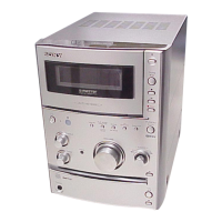
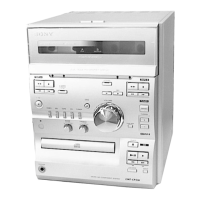
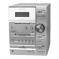
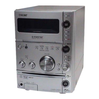
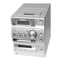
HCD-CPX11
• MAIN BOARD IC300 M3062CMEN-A14FPU0 (SYSTEM CONTROLLER)
Pin No. Pin Name I/O Description
1 MILP O CS signal output to the digital signal processor
2 MP3 REQ I REQ output to CD digital processor signal output
3 MIACK I ACK input from CD digital processor input
4 SIRCS IN/WAKE I Remote control signal input terminal
5 MP3 DATA OUT O Serial data output to MP3
6 MP3 DATA IN I Serial data input from MP3
7 MP3 CLK O Serial data transfersignal output to MP3
8 BYTE — Not used
9 CNVSS — Ground terminal
10 XCIN I Sub system clock input terminal (32.768 kHz)
11 XCOUT O Sub system clock output terminal (32.768 kHz)
System reset signal input from the reset signal generator “L”: reset
12 RESET I For several hundreds msec. after the power supply rises, “L” is input,
then it changes to “H”
13 XOUT O Main system clock output terminal (16 MHz)
14 VSS — Ground terminal
15 XIN I Main system clock input terminal (16 MHz)
16 VCC — Power supply terminal (+3.3V)
17 NMI I Non-maskable interrupt input terminal Not used
18 RDS CLK I Serial data transfer clock signal input from the RDS decoder Not used
19 CD SCOR I Subcode sync (S0+S1) detection signal input from the digital signal processor
20 AC CUT I AC off detection signal input from the reset signal generator “L”: AC cut checked
21 MP3 RST O RESET output to CD digital processor
22 MICS O CS output to the CD digital processor
23 MP3 STB O MP3 STB output signal
24 CDM LOAD-IN O Motor drive signal (close direction) output terminal
25 CDM LOAD-OUT O Motor drive signal (open direction) output terminal
26 CDM SW3 I Loading in/out detect switch input terminal “L”: loading in
27 CDM SW1 I Loading in/out detect switch input terminal “L”: loading in
28 CDM SW2 I Loading in/out detect switch input terminal “L”: loading in
29 IIC CLK I/O Communication data transfer clock signal input/output terminal Not used
30 IIC DATA I/O Communication data bus terminal Not used
31 NO USE — Not used
32 CD SENS I Internal status detection monitor input from the digital signal processor
33 CD XRST O Reset signal output to the digital signal processor and motor/coil driver “L”: reset
34 CD XTCN O CD XTCN signal output
35 CD DATA O Serial data output to the digital signal processor
36 CD XLT O Serial data latch pulse signal output to the digital signal processor
37 CD CLK O Serial data transfer clock signal output to the digital signal processor
38 CD BD-PWR O Power supply on/off control signal output for the CD section “H”: power on
39 PWR RELAY O Main system power supply on/off control signal output terminal “H”: power on
40 DIAG I Protect signal input from the power amplifier and protect detect circuit
41 ENA O Output enable control signal output to the power amplifier
42 SC DT O Serial data output to the digital audio signal processor
43 SC SHIFT O Serial data shift clock signal output to the digital audio signal processor
44 SC LATCH O Serial data latch pulse signal output to the digital audio signal processor
 Loading...