50
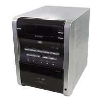
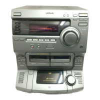
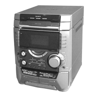
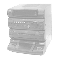
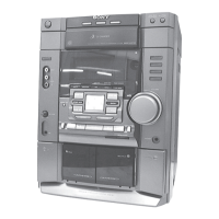
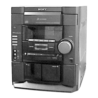
HCD-DV2D
Pin No. Pin Name I/O Description
172 Y/R/V O Video signal output
173 C/B/V O Video signal output
174 DACGNDB — Ground terminal
175 RSET I Not used in this set. Fixed at (“L”).
176 DACGNDDP — Ground terminal
177 GPCIO18 O SPDIF (DVD/CD) change signal output
178 GNDP2 — Ground terminal
179 AMCLK I AMCLK signal input from the AV decoder
180 VDDP2 — Power supply terminal (+3.3V)
181 SPDIF/AOUT3 O SPDIF DVD signal output
182 GPAIO I Not used in this set. Fixed at (“L”).
183 GNDC — Ground terminal
184 AOUT O O Signal output to the audio DAC
185 VDDC — Power supply terminal (+1.8V)
186 AOUT 1 O Not used in this set. Fixed at (“L”).
187 AOUT 2 O Not used in this set. Fixed at (“L”).
188 ALR CLK O LRCK signal output to the audio DAC
189 GNDP — Ground terminal
190 AB CLK O BCK signal output to the audio DAC
191 VDDP — Power supply terminal (+3.3V)
192 AIN — Ground terminal
193 LLCFGA O Video signal output terminal (D1/S) change signal output
194 LLCFGP O Line3 control signal output
195 GPCI017 O SDA signal output to the EEPROM
196 GPCI016 O SCL signal output to the EEPROM
197 GPCI015 O Not used in this set. Fixed at (“H”).
198 ICE TCK I Not used in this set. Fixed at (“L”).
199 ICETDI/CPCIO24 — Not used
200 IECTDO O S-VIDEO/RGB-SW control signal output
201 IECTDI O SI-SW control signal output
202 JTMS/CPCIO46 — Not used
203 JTMS/CPCIO47 O Latch enable signal output to the audio DAC
204 JTDI/PUPRD I Not used in this set. Fixed at (“H”).
205 JTDO/PUPTD I Not used in this set. Fixed at (“H”).
206 TESTMODE I Not used in this set. Fixed at (“L”).
207 GNDP — Not used
208 DUPTD I Not used in this set. Fixed at (“H”).