52
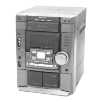
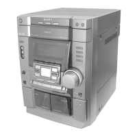
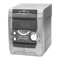
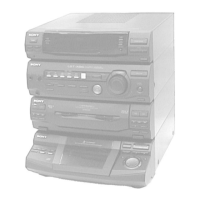
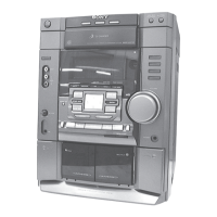
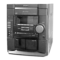
HCD-DV2D
Pin No. Pin Name I/O Description
61 MRAS1B O S-RAM low address strobe signal output
62 to 65 MA0 to 3 O S-RAM address bus
66 DVDD3 — Power supply terminal (+3.3V)
67 DVSS — Ground terminal
68 to 72 MA7 to 8 O S-RAM address bus
73 MA9 — Not used
74 MA10 — Not used
75 MOEB O S-RAM output enable signal output
76 MCASUB O S-RAM column high address strobe signal output
77 MCASLB O S-RAM column low address strobe signal output
78 to 83 HADR7 to 12 O Flash memory address bus
84 C2F O C2F signal output to the video DAC encoder
85 ROMXA O CD DATA signal output video DAC encoder
86 ROMCK O BCK signal output video DAC encoder
87 LRSY O LRCK signal output to the video DAC encoder
88 DVDD1 — Power supply terminal (+3.3V)
89 DVSS — Ground terminal
90 EMPH — Not used
91 AVRA01 O DRFO signal output to the video DAC encoder
92 AVACK0 O DACK signal output to the video DAC encoder
93 AVDACK O DACK signal output to the video DAC encoder
94 AVSCTB O DBGN signal output to the video DAC encoder
95 AVERRB O DFFR signal output to the video DAC encoder
96 to 103 AVD0 to 7 O DVD (RF) signal output to the video DAC encoder
104 EFMOUT — Not used
105 PCK — Not used
106 DVDD0 — Power supply terminal (+3.3V)
107 DVSS — Ground terminal
108 VCOCTL I FPD/PPD signal input
109 PPDO O PPD signal output
110 FPDO O FPD signal output
111 LF1 I FPD/PPD signal input
112 LF2 I FPD/PPD signal input
113 LF3 — Not used
114 PCN — Not used
115 PISET I Not used in this set. Fixed at “H”.
116 FISET I Not used in this set. Fixed at “H”.
117 CDFR I Not used in this set. Fixed at “L”.
118 DVDFR I Not used in this set. Fixed at “L”.
119 AVDD2 — Power supply terminal (+3.3V)
120 AVSS2 — Ground terminal
121 DVCP1 I Not used in this set. Fixed at “H”.
122 JVCPC1 I ADJV signal input
123 JVAO O ADJV signal output
124 JVAN I JVR signal input
125 JVRVO O JVR signal output
126 AVDD3 — Power supply terminal (+3.3V)
127 AVSS — Ground terminal
128 VPDO O VPD signal output