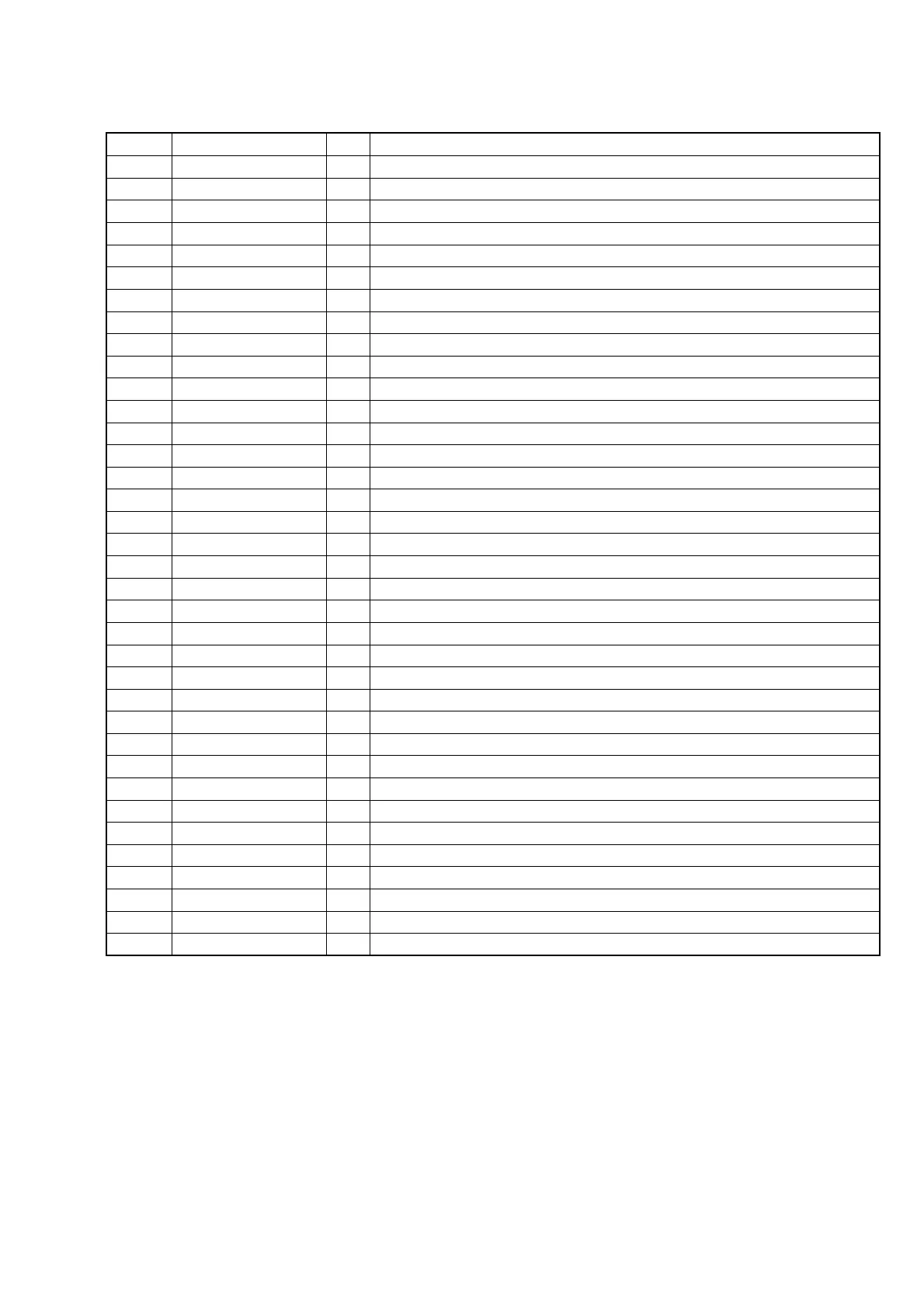
53
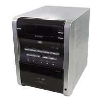
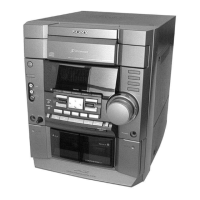
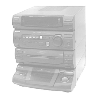
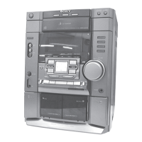
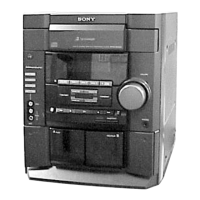
HCD-DV2D
Pin No. Pin Name I/O Description
129 VRPFR I Not used in this set. Fixed at “H”.
130 VCOCTL I VPD signal input
131 DVDD0 — Power supply terminal (+3.3V)
132 DVSS — Ground terminal
133 DVDD2 — Power supply terminal (+3.3V)
134 XIN I System clock input (16.9344MHz)
135 XOUT O System clock output (16.9344MHz)
136 DVSS — Ground terminal
137 X16MIO O AMCLK signal output to the video DAC encoder
138 TEST2 — Ground terminal
139 DVDCKIO — Ground terminal
140 SYEO(EFLO) — Not used.
141 FSEO(FSX) — Not used.
142 DOUT O SPDIF CD signal output
143 DVDD1 — Power supply terminal (+3.3V)
144 DVSS — Ground terminal
145 to 148 MD8 to 11 I/O S-RAM data bus
149 DVSS — Ground terminal
150 to 153 MD12 to 15 I/O S-RAM data bus
154 DVSS — Ground terminal
155 DVDD3 — Power supply terminal (+3.3V)
156 to 159 MD0-3 I/O S-RAM data bus
160 DVDD3 — Power supply terminal (+3.3V)
161 to 164 MD4 to 7 I/O S-RAM data bus
165 DVDD1 — Power supply terminal (+3.3V)
166 DVSS — Ground terminal
167 DVD CD O DVD/CD change control signal output
168 DEFECTO O RFAMP tracking hold control signal output
169 WRO O WRO signal output
170 XHTR O Tracking band control signal output to the RF AMP
171 LDON1 O APC2 laser control signal output to the RF AMP
172 LDON2 O APC1 laser control signal output to the RF AMP
173 TESIO — Not used.
174 HFLIO — Not used.
175 DVDD0 — Power supply terminal (+3.3V)
176 DVSS — Ground terminal