HT-NT5
61
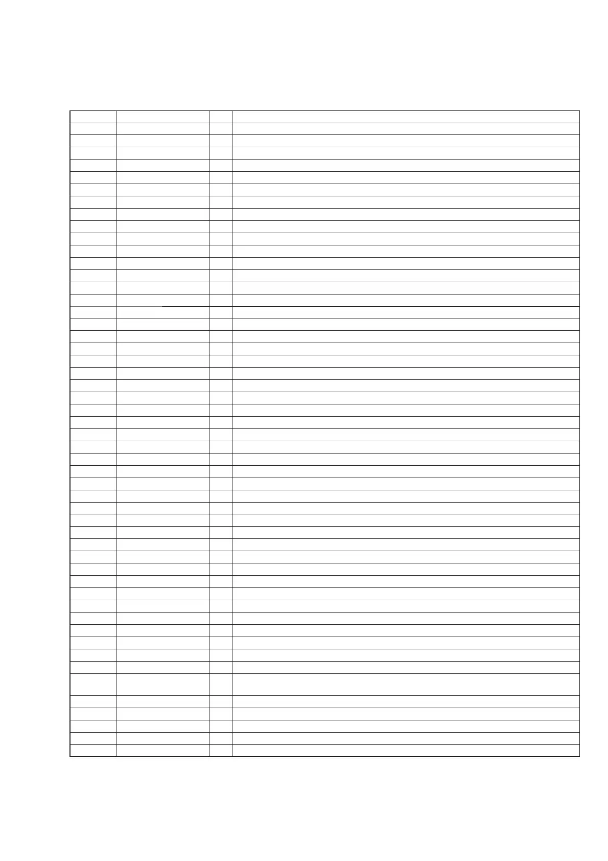
• IC Pin Function Description
AMP BOARD IC6005 CXD3776ER-T9 (AUDIO CODEC)
Pin No. Pin Name I/O Description
1 SDIN1 I Audio signal (for woofer) input from the SoC
2 SDIN2 I Audio signal input terminal Not used
3 LRCKO I/O L/R sampling clock signal input/output terminal Not used
4 BCKO I/O Bit clock signal input/output terminal Not used
5, 6 SDOUT1, SDOUT2 O Audio signal output terminal Not used
7 FS256O O 256fs clock signal output terminal Not used
8 XLDO_EN I LDO enable signal input terminal “L”: LDO on Fixed at “L” in this unit
9 MCKO O Master clock signal output terminal Not used
10 XTO O System clock output terminal Not used
11 XTI I System clock input terminal (49.152 MHz)
12 SCL I I2C clock signal input from the system controller
13 SDA I/O Two-way I2C data bus with the system controller
14 XRESET I Reset signal input from the system controller “L”: reset
15 XINT O Interrupt signal output to the system controller
16 OUT1PL_NR O PWM audio signal (R-ch negative) output to the digital power amplifi er
17 OUT1NL_PR O PWM audio signal (R-ch positive) output to the digital power amplifi er
18 VDDPWM1 - Power supply terminal (+3.3V)
19 GNDPWM1 - Ground terminal
20 OUT1PR_PL O PWM audio signal (L-ch positive) output to the digital power amplifi er
21 OUT1NR_NL O PWM audio signal (L-ch negative) output to the digital power amplifi er
22 PWMOUT2PL O PWM audio signal (L-ch positive) output terminal Not used
23 PWMOUT2NL O PWM audio signal (L-ch negative) output terminal Not used
24 VDDPWM2 - Power supply terminal (+3.3V)
25 GNDPWM2 - Ground terminal
26 PWMOUT2PR O PWM audio signal (R-ch positive) output terminal Not used
27 PWMOUT2NR O PWM audio signal (R-ch negative) output terminal Not used
28 ADDSEL I I2C address selection signal input terminal Fixed at “L” in this unit
29 TST_MODE I Test mode setting terminal Fixed at “L” in this unit
30 AVDD2R - Power supply terminal (+3.3V)
31 AOUT2R O Audio signal (R-ch) output terminal Not used
32, 33 AGND2R, AGND2L - Ground terminal
34 AOUT2L O Audio signal (L-ch) output terminal Not used
35, 36 AVDD2L, AVDD1R - Power supply terminal (+3.3V)
37 AOUT1R O Audio signal (R-ch) output terminal Not used
38, 39 AGND1R, AGND1L - Ground terminal
40 AOUT1L O Audio signal (L-ch) output terminal Not used
41 AVDD1L - Power supply terminal (+3.3V)
42 VQ O Reference voltage output terminal
43 VCOM I Reference voltage fi lter input terminal
44 AINNL I Audio signal (L/R-ch mix) input from the digital power amplifi er
45 AINPL I Audio signal (L-ch negative) input from the digital power amplifi er
46 AGNDAD - Ground terminal
47 AVDDAD - Power supply terminal (+3.3V)
48 AINNR I Audio signal (L/R-ch mix) input from the digital power amplifi er
49 AINPR I Audio signal (R-ch negative) input from the digital power amplifi er
50, 51
PSENSEIN,
TSENSEIN
I Input terminal for SAR A/D converter Not used
52 DGND - Ground terminal
53 VD_FILT O LDO fi lter connection terminal
54 DVDD - Power supply terminal (+3.3V)
55 LRCKI I L/R sampling clock signal input from the SoC
56 BCKI I Bit clock signal input from the SoC
 Loading...