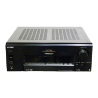
STR-DA5300ES
22
STR-DA5300ES
• Note for Printed Wiring Boards and Schematic Diagrams
• DSP board is multi-layer printed board.
However, the patterns of intermediate-layers have not been
included in this diagrams.
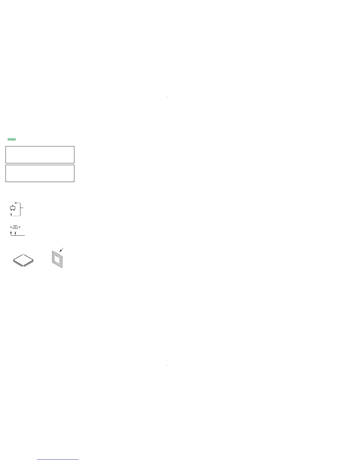
• Indication of transistor
Note on Schematic Diagram:
• All capacitors are in µF unless otherwise noted. (p: pF)
50 WV or less are not indicated except for electrolytics
and tantalums.
• All resistors are in Ω and
1
/
4
W or less unless otherwise
specified.
•
f : internal component.
• C : panel designation.
• A : B+ Line.
• B : B– Line.
• Voltages are dc with respect to ground under no-signal
(detuned) conditions.
no mark : TUNER
• Voltages are taken with a VOM (Input impedance 10 MW).
Voltage variations may be noted due to normal produc-
tion tolerances.
F : AUDIO (ANALOG)
J : AUDIO (DIGITAL)
• The voltage and waveform of CSP (chip size package)
cannot be measured, because its lead layout is different
from that of conventional IC.
• Abbreviation
CND : Canadian model
ECE : Russian and Ukrainian models
Note on Printed Wiring Board:
• X : parts extracted from the component side.
• Y : parts extracted from the conductor side.
•
f : internal component.
• : Pattern from the side which enables seeing.
(The other layers' patterns are not indicated.)
Caution:
Pattern face side: Parts on the pattern face side seen from
(Conductor Side) the pattern face are indicated.
Parts face side: Parts on the parts face side seen from
(Component Side) the parts face are indicated.
Caution:
Pattern face side: Parts on the pattern face side seen from
(Side B) the pattern face are indicated.
Parts face side: Parts on the parts face side seen from
(Side A) the parts face are indicated.
Lead layout of conventional IC CSP (chip size package)
• Lead Layouts
2. DIAGRAMS
C
B
These are omitted.
E
Q
B
These are omitted.
CE
Q
surfac