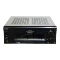
STR-DA5300ES
4545
STR-DA5300ES
• Note for Printed Wiring Boards and Schematic Diagrams
• D-VIDEO and DSP boards are multi-layer printed board.
However, the patterns of intermediate-layers have not been
included in this diagrams.
• Indication of transistor
C
B
These are omitted.
E
Q
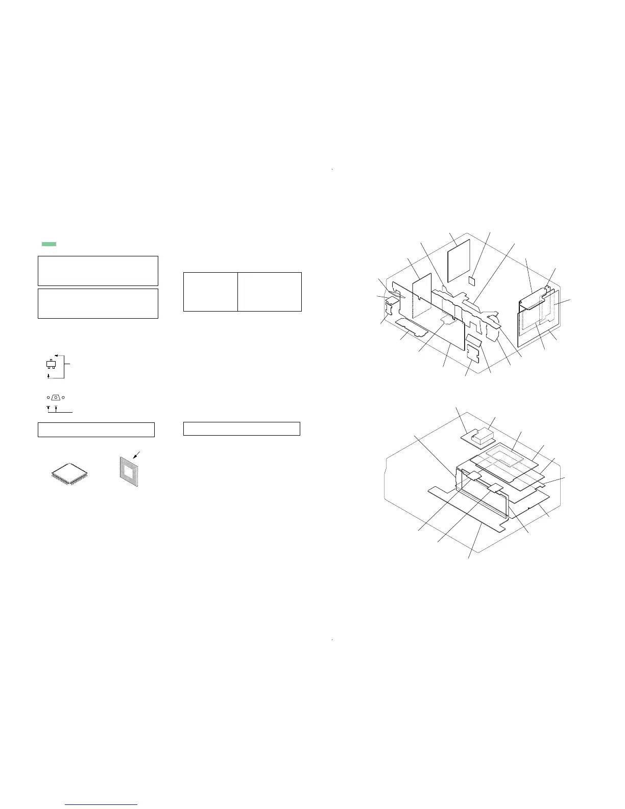
• Circuit Boards Location
Note on Schematic Diagram:
• All capacitors are in µF unless otherwise noted. (p: pF)
50 WV or less are not indicated except for electrolytics
and tantalums.
• All resistors are in Ω and
1
/
4
W or less unless otherwise
specified.
•
f : internal component.
• 2 : nonflammable resistor.
• C : panel designation.
• A : B+ Line.
• B : B– Line.
• H : adjustment for repair.
• Voltages and waveforms are dc with respect to ground
under no-signal (detuned) conditions.
– A-VIDEO and S-VIDEO boards –
no mark : VIDEO 1 mode
– Other boards –
no mark : TUNER
• Voltages are taken with a VOM (Input impedance 10 MW).
Voltage variations may be noted due to normal produc-
tion tolerances.
• Waveforms are taken with a oscilloscope.
Voltage variations may be noted due to normal produc-
tion tolerances.
• Circled numbers refer to waveforms.
• Signal path.
F : AUDIO (ANALOG)
J : AUDIO (DIGITAL)
E : VIDEO
Note on Printed Wiring Board:
• X : parts extracted from the component side.
• Y : parts extracted from the conductor side.
•
f : internal component.
• : Pattern from the side which enables seeing.
(The other layers' patterns are not indicated.)
Caution:
Pattern face side: Parts on the pattern face side seen from
(Conductor Side) the pattern face are indicated.
Parts face side: Parts on the parts face side seen from
(Component Side) the parts face are indicated.
Caution:
Pattern face side: Parts on the pattern face side seen from
(Side B) the pattern face are indicated.
Parts face side: Parts on the parts face side seen from
(Side A) the parts face are indicated.
B
These are omitted.
CE
Q
Note:
The components identi-
fied by mark 0 or dotted
line with mark 0 are criti-
cal for safety.
Replace only with part
number specified.
Note:
Les composants identifiés par
une marque 0 sont critiques
pour la sécurité.
Ne les remplacer que par une
pièce portant le numéro
spécifié.
surfac
Lead layout of conventional IC CSP (chip size package)
• Lead Layouts
* Replacement of IC3601on the D-VIDEO board used in
this set requires a special tool.
• The voltage and waveform of CSP (chip size package)
cannot be measured, because its lead layout is different
from that of conventional IC.
• Abbreviation
CND : Canadian model
ECE : Russian and Ukrainian models
* Replacement of IC3601on the D-VIDEO board used in
this set requires a special tool.
SP-TM board
TUNER (FM/AM)
PROTECTOR (SURR) board
KEY 1 board
PROTECTOR (SB) board
AC board
A-VIDEO board
ANALOG board
S-VIDEO board
D-VIDEO board
MAIN board
E-VOL board
CONNECTOR 2 board
A-CLASS AMP board
POWER AMPLIFIER board
CONNECTOR 1 board
D-CONNECT board
CONTROL board
FLI-1.8REG board
PROTECTOR (F-C) board
TEMPERATURE
DETECTION board
VIDEO3 board
MAIN VOL board
DISPLAY board
DSP board
BIAS board
CIS board
DIGITAL board
AC SW board
DC-DC board
SPSW board
MIC board
Ver. 1.1