STR-DA5500ES
131
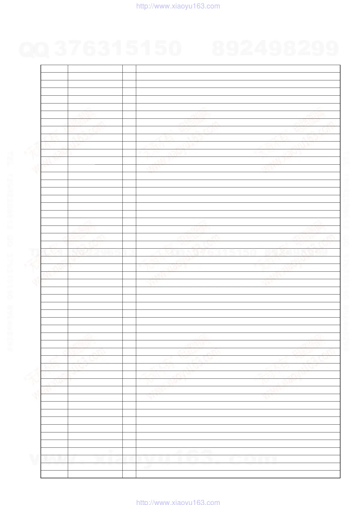
• IC Pin Function Description
D-AUDIO BOARD IC2003 EP2C5T144C8N (FIELD PROGRAMMABLE GATE ARRAY)
Pin No. Pin Name I/O Description
1
∗ASDO
O Serial data output to the fl ash memory
2
∗nCSO
O Chip select signal output to the fl ash memory
3 MUTEOUT O Muting control signal output terminal
4 AMCKOUT O Audio master clock signal output to the D/A converter (for audio section)
5 VCCIO1 - Power supply terminal (+3.3V)
6 GND - Ground terminal
7 LRCKOUT O L/R sampling clock signal output for digital audio signal to the lip sync adjust
8 - - Not used
9 BCKOUT O Bit clock signal output for digital audio signal to the lip sync adjust
10
∗TDO
O Data output terminal (for JTAG) Not used
11
∗TMS
I Mode selection signal input terminal (for JTAG) Not used
12
∗TCK
I Clock signal input terminal (for JTAG) Not used
13
∗TDI
I Data input terminal (for JTAG) Not used
14
∗DATA0
I Serial data input from the fl ash memory
15
∗DCLK
O Serial data transfer clock signal output to the fl ash memory
16
∗nCE
I Chip enable signal input terminal Not used
17 MCLKIN I Master clock signal input from the digital audio interface receiver or HDMI receiver
18 BCKIN I Bit clock signal input for digital audio signal from the DSP2
19 GND - Ground terminal
20
∗nCONFIG
I Confi guration control signal input terminal Not used
21 XRESET I Reset signal input from the system controller “L”: reset
22 AMCKIN I Audio master clock signal input terminal
23 VCCIO1 - Power supply terminal (+3.3V)
24 SD0OUT O Digital audio signal (front L/R) output to the lip sync adjust
25 SD1OUT O Digital audio signal (surround L/R) output to the lip sync adjust
26 - - Not used
27 SD2OUT O Digital audio signal (center, subwoofer) output to the lip sync adjust
28 SD3OUT O Digital audio signal (surround back L/R) output to the lip sync adjust
29 VCCIO1 - Power supply terminal (+3.3V)
30 - - Not used
31 LRCKIN I L/R sampling clock signal input for digital audio signal from the DSP2
32 - - Not used
33 GND - Ground terminal
34 GND_PLL1 - Ground terminal (for PLL)
35 VCCD_PLL1 - Power supply terminal (+1.2V) (digital system) (for PLL)
36 GND_PLL1 - Ground terminal (for PLL)
37 VCCA_PLL1 - Power supply terminal (+1.2V) (analog system) (for PLL)
38 GNDA_PLL1 - Ground terminal (analog system) (for PLL)
39 GND - Ground terminal
40 SD0IN I Digital audio signal (front L/R) input from the DSP2
41 - - Not used
42 SD1IN I Digital audio signal (surround L/R) input from the DSP2
43 SD2IN I Digital audio signal (center, subwoofer) input from the DSP2
44 - - Not used
45 SD3IN I Digital audio signal (surround back L/R) input from the DSP2
46 VCCIO4 - Power supply terminal (+3.3V)
47 I2CADRS0 - Not used
48 I2CADRD1 - Not used
49 GND - Ground terminal
50 VCCINT - Power supply terminal (+1.2V)
51 SDRAM - Not used
52, 53 - - Not used
54 VCCIO4 - Power supply terminal (+3.3V)
w
w
w
.
x
i
a
o
y
u
1
6
3
.
c
o
m
Q
Q
3
7
6
3
1
5
1
5
0
9
9
2
8
9
4
2
9
8
T
E
L
1
3
9
4
2
2
9
6
5
1
3
9
9
2
8
9
4
2
9
8
0
5
1
5
1
3
6
7
3
Q
Q
TEL 13942296513 QQ 376315150 892498299
TEL 13942296513 QQ 376315150 892498299
http://www.xiaoyu163.com
http://www.xiaoyu163.com