STR-DA5500ES
154
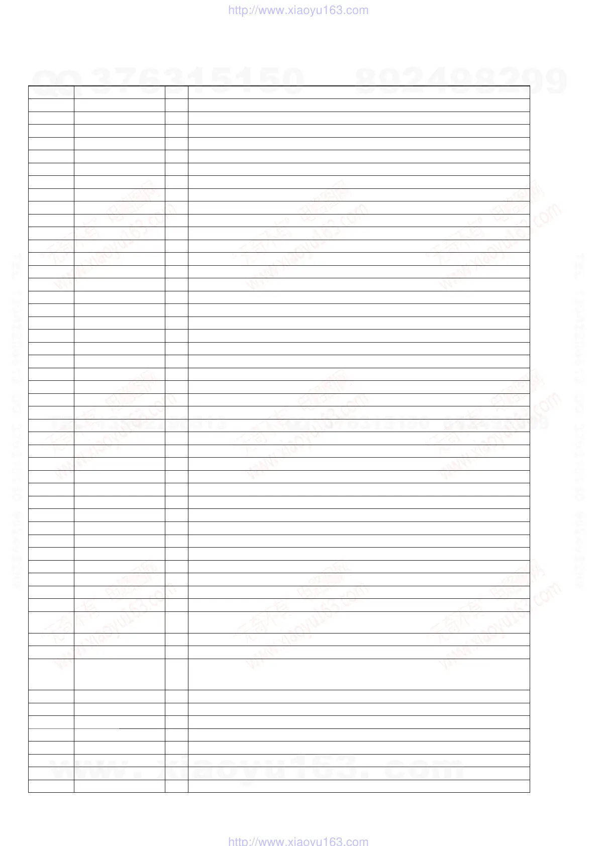
D-VIDEO BOARD IC3604 YGV629-VZ (OSD CONTROLLER)
Pin No. Pin Name I/O Description
1 PLLVDD - Power supply terminal (+3.3V)
2 FILTER I Filter connection terminal for internal PLL
3 PLLVSS - Ground terminal
4 NC - Not used
5 to 10 PLLCTL5 to PLLCTL0 I PLL setting terminal
11 DTCKS_N I Clock signal input terminal Not used
12 DTCK_IN I Clock signal input terminal Not used
13 VSS - Ground terminal
14 VDD - Power supply terminal (+3.3V)
15 to 22 D0 to D7 I/O Two-way data bus with the video system controller and S-RAM
23 WAIT_N O Wait signal output to the video system controller
24 READY_N O Ready signal output terminal Not used
25 INT_N O Interrupt signal output to the video system controller
26 VDD - Power supply terminal (+3.3V)
27 VSS - Ground terminal
28 CS_N I Chip enable signal input from the video system controller
29 WR_N I Write enable signal input from the video system controller
30 RD_N I Read enable signal input from the video system controller
31 to 33 PS2 to PS0 I Address signal input from the video system controller
34 SDOUT O Serial data output terminal Not used
35 SDIN I Serial data input terminal Not used
36 SCS_N I Chip select signal input terminal Not used
37 SCLK I Serial data transfer clock signal input terminal Not used
38 SER_N I CPU interface selection setting terminal Fixed at “H” in this set
39 RESET_N I Reset signal input from the video system controller “L”: reset
40 VSS - Ground terminal
41 VDD - Power supply terminal (+3.3V)
42 MA0 O Address signal output terminal Not used
43 to 47 MA1 to MA5 O Address signal output to the fl ash memory
48 VSS - Ground terminal
49 to 54 MA6 to MA11 O Address signal output to the fl ash memory
55 VDD - Power supply terminal (+3.3V)
56 VSS - Ground terminal
57 to 62 MA12 to MA17 O Address signal output to the fl ash memory
63 VSS - Ground terminal
64 to 70 MA18 to MA24 O Address signal output to the fl ash memory
71 VDD - Power supply terminal (+3.3V)
72 VSS - Ground terminal
73 MWE_N O Write enable signal output to the fl ash memory
74 MOE_N O Output enable signal output to the fl ash memory
75 to 80
MD15, MD7, MD14,
MD6, MD13, MD5
I/O Two-way data bus with the fl ash memory
81 VSS - Ground terminal
82 VDD - Power supply terminal (+3.3V)
83 to 90
MD12, MD4, MD11,
MD3, MD10, MD2,
MD9, MD1
I/O Two-way data bus with the fl ash memory
91 VSS - Ground terminal
92 VDD - Power supply terminal (+3.3V)
93, 94 MD8, MD0 I/O Two-way data bus with the fl ash memory
95 RAHZ_N - Not used
96 to 98 XTEST2 to XTEST0 - Not used
99 VSIN_N I Vertical sync signal input terminal Not used
100 HSIN_N I Horizontal sync signal input terminal Not used
101 NC - Not used
w
w
w
.
x
i
a
o
y
u
1
6
3
.
c
o
m
Q
Q
3
7
6
3
1
5
1
5
0
9
9
2
8
9
4
2
9
8
T
E
L
1
3
9
4
2
2
9
6
5
1
3
9
9
2
8
9
4
2
9
8
0
5
1
5
1
3
6
7
3
Q
Q
TEL 13942296513 QQ 376315150 892498299
TEL 13942296513 QQ 376315150 892498299
http://www.xiaoyu163.com
http://www.xiaoyu163.com