Connector
Pin
number
Pin name Signal name STM32U5 pin Function
CN1
B7 USB_N - PA11 USB diff pair M
B9 VBUS VBUS_C - Power
B12 GND GND - Ground
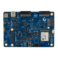
7.6 NOR flash, PSRAM, and EEPROM memories
The MX25LM51245GXDI00 512‑Mbit Octo‑SPI NOR flash from Macronix, the APS6408L‑3OB‑BA 64‑Mbit
Octo‑SPI PSRAM from AP Memory, and the M24256‑DFMC6TG I
2
C EEPROM from STMicroelectronics are
available on the B-U585I-IOT02A Discovery kit.
The M24256‑DFMC6TG is connected on ISC2 (PH4, PH5) with the 0xAC address for a write operation and 0xAD
for a read operation.
In option, it is possible to mount a Quad-SPI SRAM APS1604M‑3SQR‑SN to replace the PSRAM.
Table 10. Octo‑SPI flash I/O configuration
I/O Configuration
PF0 SIO0 (OCTOSPI.F_IO0)
PF1 SIO1 (OCTOSPI.F_IO1)
PF2 SIO2 (OCTOSPI.F_IO2)
PF3 SIO3 (OCTOSPI.F_IO3)
PH9 SIO4 (OCTOSPI.F_IO4)
PH10 SIO5 (OCTOSPI.F_IO5)
PH11 SIO6 (OCTOSPI.F_IO6)
PH12 SIO7 (OCTOSPI.F_IO7)
PF12 DQS (OCTOSPI.F_DQS)
PF4 SCLK (OCTOSPI.F_CLK_P)
PI5 NCS (OCTOSPI.F_NCS)
NRST NRESET (OCTOSPI_FLASH_RESET)
Table 11. Octo‑SPI RAM I/O configuration
I/O
Configuration
PF8 DQ0/SIO0 (OCTOSPI.R_IO0)
PF9 DQ1/SIO1 (OCTOSPI.R_IO1)
PF7 DQ2/SIO2 (OCTOSPI.R_IO2)
PF6 DQ3/SIO3 (OCTOSPI.R_IO3)
PH2 DQ4 (OCTOSPI.R_IO4)
PI0 DQ5 (OCTOSPI.R_IO5)
PC3 DQ6 (OCTOSPI.R_IO6)
PD7 DQ7 (OCTOSPI.R_IO7)
PE3 DQS (OCTOSPI.R_DQS)
PB10 CLK/SCLK (OCTOSPI.R_CLK_P)
PB11 CE (NCS) (OCTOSPI.R_NCS)
NRST RST (OCTOSPI_SRAM_RESET)
UM2839
NOR flash, PSRAM, and EEPROM memories
UM2839 - Rev 4
page 22/54