EasyManua.ls Logo

ST STM32F3 Series User Manual

ST STM32F3 Series
262 pages
To Next Page IconTo Next Page
To Previous Page IconTo Previous Page
Page #215 background imageLoading...
Page #215 background image
PM0214 Rev 10 215/262
PM0214 Core peripherals
261
4.3.7 Interrupt priority register x (NVIC_IPRx)
Address offset: 0x400 + 0x04 * x, (x = 0 to 59)
Reset value: 0x0000 0000
Required privilege: Privileged
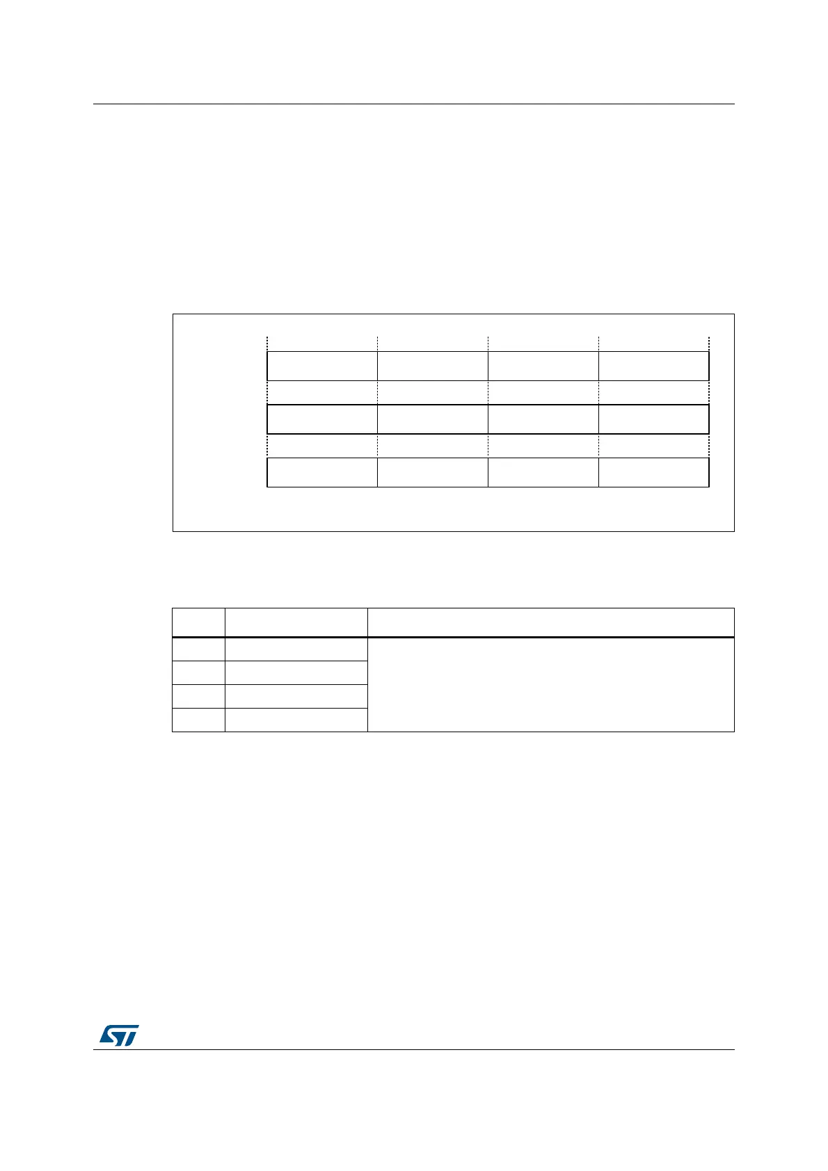
The NVIC_IPRx (x = 0 to 59) byte-accessible registers provide 8-bit priority fields IP[N]
(N = 0 to 239) for each of the 240 interrupts. Every register holds four IP[N] fields of the
CMSIS interrupt priority array, as shown in Figure 19.
Figure 19. Mapping of IP[N] fields in NVIC_IPRx registers
The following table shows the bit assignment of any NVIC_IPRx register. Each IP[N] field
order can be expressed as N = 4 * x + byte offset.
See Interrupt set-enable register x (NVIC_ISERx) on page 210 for a view of the interrupt
priorities from the software perspective.
Note: The number of interrupts is product-dependent. Refer to reference manual/datasheet of
relevant STM32 product for related information.
Table 47. NVIC_IPRx bit assignment
Bits Name Function
[31:24] Priority, byte offset = 3
Each priority field holds a priority value, 0-255. The lower the
value, the greater the priority of the corresponding interrupt. The
processor implements only bits[7:4] of each field, bits[3:0] read
as zero and ignore writes.
[23:16] Priority, byte offset = 2
[15:8] Priority, byte offset = 1
[7:0] Priority, byte offset = 0
MSv47990V1
IP[3] IP[2] IP[1] IP[0]
IP[4x+3] IP[4x+2] IP[4x+1] IP[4x]
NVIC_IPR0
NVIC_IPRx
IP[239] IP[238] IP[237] IP[236]
NVIC_IPR59
0781516232431

Table of Contents

Question and Answer IconNeed help?

Do you have a question about the ST STM32F3 Series and is the answer not in the manual?

ST STM32F3 Series Specifications

General IconGeneral
SeriesSTM32F3
CoreARM Cortex-M4
Max CPU Frequency72 MHz
Operating Voltage2.0 V to 3.6 V
GPIO PinsUp to 80
TimersAdvanced-control, general-purpose, basic timers
ADC12-bit
DAC12-bit
Communication InterfacesUSART, SPI, I2C, CAN, USB
Operating Temperature-40°C to 85°C
PackageLQFP, UFQFPN, WLCSP

Summary

Introduction

1 About this document

1.1 Typographical conventions

Conventions used in the document for formatting text and code elements.

1.2 List of abbreviations for registers

Abbreviations used in register descriptions.

1.3 About the STM32 Cortex-M4 processor and core peripherals

Overview of the processor's features and integrated peripherals.

2 The Cortex-M4 processor

2.1 Programmers model

Describes the programmer's model, processor modes, privilege levels, and stacks.

2.2 Memory model

Details the processor memory map, access behavior, and bit-banding features.

2.3 Exception model

Explains the exception model, states, types, handlers, and priorities.

2.4 Fault handling

Details fault types, escalation, status registers, and lockup.

2.5 Power management

Describes mechanisms for entering and waking up from sleep modes.

3 The STM32 Cortex-M4 instruction set

3.1 Instruction set summary

Overview of the instruction set and supported instructions.

3.2 CMSIS intrinsic functions

CMSIS intrinsic functions for generating Cortex-M4 instructions.

3.3 About the instruction descriptions

Explains how instruction descriptions are presented in the document.

3.4 Memory access instructions

Details instructions for accessing memory.

3.5 General data processing instructions

Covers general-purpose data processing instructions.

3.6 Multiply and divide instructions

Describes instructions for multiplication and division operations.

3.7 Saturating instructions

Explains instructions that perform saturating arithmetic.

3.8 Packing and unpacking instructions

Instructions for packing and unpacking data.

3.9 Bitfield instructions

Instructions for operating on bitfields within registers.

3.10 Floating-point instructions

Instructions for floating-point operations using the FPU.

3.11 Miscellaneous instructions

Other Cortex-M4 instructions not categorized elsewhere.

4 Core peripherals

4.1 About the STM32 Cortex-M4 core peripherals

Overview of core peripherals and their memory map in the PPB.

4.2 Memory protection unit (MPU)

Details the MPU's functionality for memory protection and region management.

4.3 Nested vectored interrupt controller (NVIC)

Describes the NVIC's support for interrupts, priorities, and tail-chaining.

4.4 System control block (SCB)

Provides system implementation info and control for exceptions.

4.5 SysTick timer (STK)

Details the SysTick timer, its registers, and usage hints.

4.6 Floating point unit (FPU)

Explains the FPU's functionality, registers, and enabling.

5 Revision history

Related product manuals