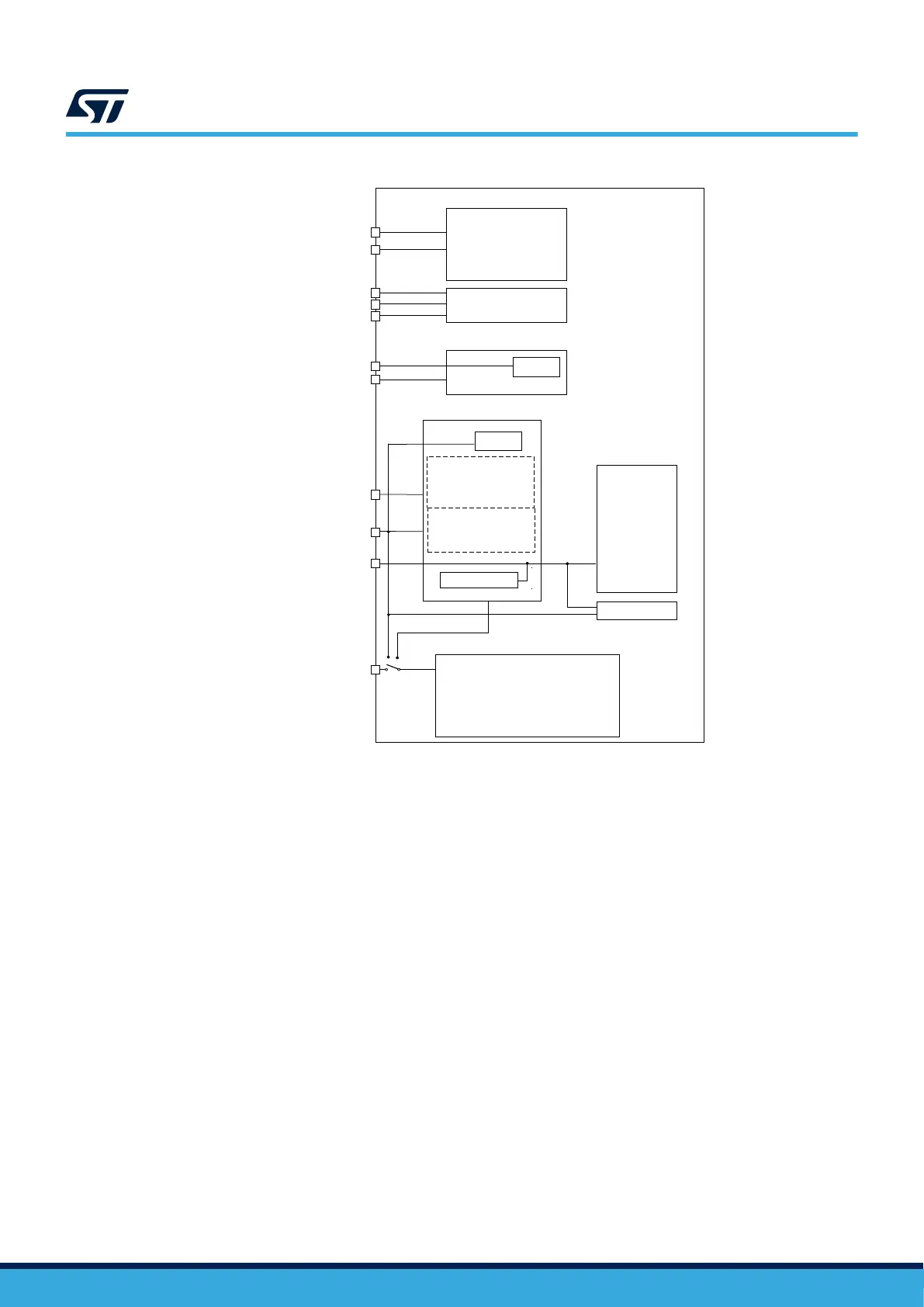
Figure 6. STM32U5F/5G/59/5Axxx power supply overview (without SMPS)
DT66058V2
Core
SRAM1
SRAM2
SRAM3
SRAM4
SRAM5
SRAM6
(2)
Digital
peripherals
LSE crystal 32kHz oscillator
LSI 32 kHz oscillator
Backup registers
RCC_BDCR and PWR_BDCR1 registers
RTC
TAMP
BKPSRAM
V
DDA
domain
Backup domain
Standby circuitry
(Wake-up logic, IWDG)
Low-voltage detector
I/O ring
V
CORE
domain
Temperature sensor
Reset block
3 x PLL
Internal RC oscillators
Flash memory
VDDUSB
VDDIO2
V
DDIO1
I/O ring
PG[15:2]
V
DDIO2
VDDA
VSSA
VDD11USB
(1)
VSS
V
DDIO2
domain
V
DD
domain
V
CORE
VSS
VDD
VBAT
VCAP
A/D converters
Comparators
D/A converters
Operational amplifiers
Voltage reference buffer
USB transceiver
VSS
(1) Only available on specific packages.
(2) Only for STM32U5Fx/5Gx devices.
LDO regulator
V
SW
In devices without SMPS, the V
DD
supply source feeds the I/Os and system analog peripherals (such as PLLs
and reset block). The V
CORE
power supply for digital peripherals and memories is generated from the LDO.
Note: If the selected package has the SMPS step-down converter option but the SMPS is not used by the application
(and the embedded LDO is used instead), the SMPS power supply pins must be set as follows:
• VDDSMPS and VLXSMPS connected to VSS
• VDD11 pins connected to VSS through two 2.2 µF capacitors as in normal mode
2.1.1 Independent analog peripherals supply
To improve ADC and DAC conversion accuracy and to extend the supply flexibility, the analog peripherals have
an independent power supply that can be separately filtered and shielded from noise on the PCB.
The voltage supply input of the analog peripherals is available on a separate VDDA pin. An isolated supply
ground connection is provided on VSSA pin.
The V
DDA
supply voltage can be different from V
DD
. After reset, the analog peripherals supplied by V
DDA
are
logically and electrically isolated and therefore are not available. The isolation must be removed before using
these peripherals, by setting the ASV bit in PWR_SVMCR, once the V
DDA
supply is present.
The V
DDA
supply can be monitored by analog voltage monitors (AVM), and compared with two thresholds
(1.6 V for AVM1 or 1.8 V for AVM2). For more details, refer to the device datasheet and section Peripheral voltage
monitoring (PVM) of document [1].
When a single supply is used, the VDDA pin can be externally connected to the same V
DD
supply, through an
external filtering circuit, to ensure a noise-free V
DD
reference voltage.
AN5373
Power supplies
AN5373 - Rev 6
page 10/47
 Loading...


