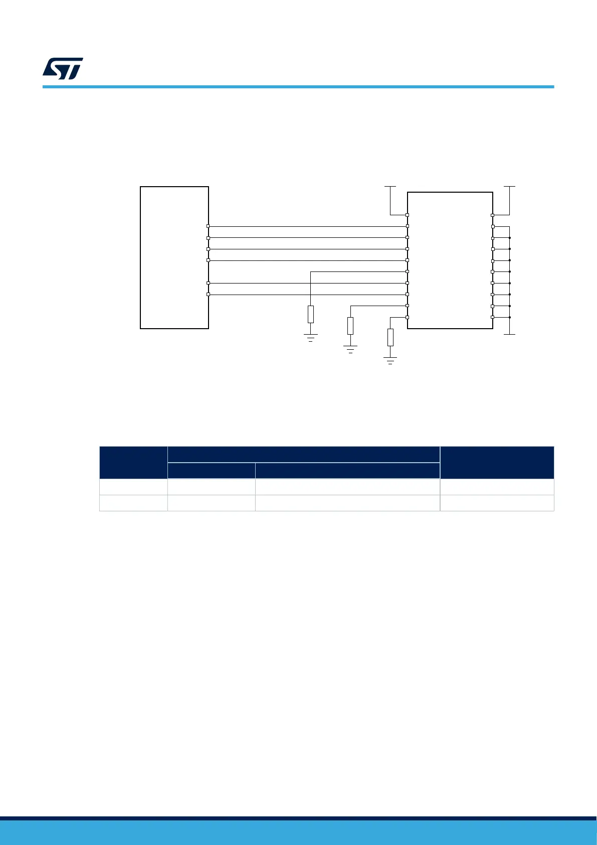
6.2.4 SWJ-DP connection with standard JTAG connector
The figure below shows the connection between the device and a standard JTAG connector.
Figure 15. JTAG connector implementation
DT64362V1
V
DD
STM32U5 MCU
nJTRST
JTDI
JTMS/SWDIO
JTCK/SWCLK
JTDO
nRST
(1) VTREF
(3) nTRST
(5) TDI
(7) TMS
(9) TCK
(11) RTCK
(15) nSRST
(19) DBGACK
10 kΩ
(2)
(4)
(6)
(8)
(10)
(12)
(14)
(16)
(18)
(20)
JTAG connector
10 kΩ
10 kΩ
(17) DBGRQ
(13) TDO
V
DD
V
SS
Connector 2 x 10
6.3 Serial-wire debug (SWD) pin assignment
The same SWD pin assignment, detailed in the table below, is available on all packages.
Table 8. SWD port pins
SWD pin
SWD port
Pin assignment
Type Debug assignment
SWDIO
Input/Output Serial-wire data input/output
PA13
SWCLK Input Serial-wire clock PA14
After reset, the pins used for the SWD are assigned as dedicated pins that can be immediately used by the
debugger host.
However, the MCU offers the possibility to disable the SWD, therefore releasing the associated pins for GPIO
use.
For more details on how to disable SWD port, refer to section I/O pin alternate function multiplexer and mapping
of document [1].
6.3.1 Internal pull-up and pull-down on SWD pins
Once the user software releases the SWD I/O, the GPIO controller takes control of it. The reset states of the
GPIO control registers put the I/Os in the equivalent states:
• SWDIO: alternate function pull-up
• SWCLK: alternate function pull-down
Having embedded pull-up and pull-down resistors removes the need to add external resistors.
AN5373
Serial-wire debug (SWD) pin assignment
AN5373 - Rev 6
page 32/47
 Loading...


