6.2.2 Flexible SWJ-DP pin assignment
After reset (SYSRESETn or PORESETn), all five pins used for the SWJ-DP are assigned as dedicated pins that
are immediately usable by the debugger host.
Note: The trace outputs are not assigned except if explicitly programmed by the debugger host.
The table below shows the different possibilities for releasing some pins (refer to document [1] for more details).
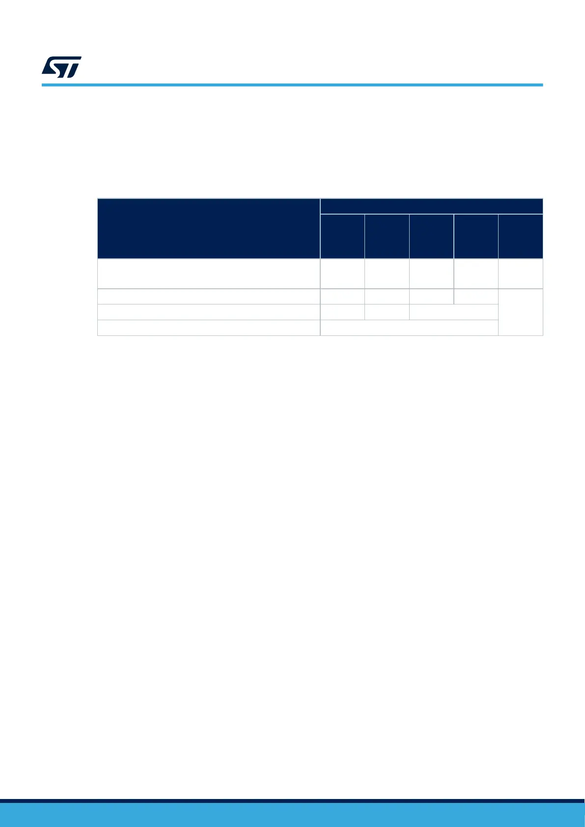
Table 7. SWJ-DP I/O pin availability
Available debug ports
SWJ-DP I/O pin assigned
PA13 /
JTMS/
SWDIO
PA14 /
JTCK/
SWCLK
PA15 /
JTDI
PB3 /
JTDO
PB4/
JNTRST
Full SWJ‑DP (JTAG‑DP + SW‑DP)
Reset state
X X X X X
Full SWJ‑DP (JTAG‑DP + SW‑DP) but without JNTRST X X X X
-JTAG-DP disabled and SW-DP enabled X X -
JTAG-DP disabled and SW-DP disabled Released
6.2.3 Internal pull-up and pull-down resistors on JTAG pins
The JTAG input pins must not be floating since they are directly connected to flip-flops that control the debug
mode features. Special care must be taken with the SWCLK/TCK pin that is directly connected to the clock of
some of these flip-flops.
To avoid any uncontrolled I/O levels, the devices embed the following internal resistors on the JTAG input pins:
• JNTRST: internal pull-up
• JTDI: internal pull-up
• JTMS/SWDIO: internal pull-up
• TCK/SWCLK: internal pull-down
Once the user software releases the JTAG I/O, the GPIO controller takes the control again, and the software can
then use these I/Os as standard GPIOs. The reset states of the GPIO control registers put the I/Os in the
following equivalent states:
• JNTRST: input pull-up
• JTDI: input pull-up
• JTMS/SWDIO: input pull-up
• JTCK/SWCLK: input pull-down
• JTDO: input floating
Note: The JTAG IEEE standard recommends adding pull-up resistors on TDI, TMS, and nTRST, but there is no special
recommendation for TCK. However, for the devices, an integrated pull-down resistor is used for JTCK. Having
embedded pull-up and pull-down resistors removes the need to add external resistors.
AN5373
Pinout and debug port pins
AN5373 - Rev 6
page 31/47

 Loading...


