2.3 Power supply sequence between V
DDA
, V
DDUSB
, V
DDIO2
, and V
DD
2.3.1 Power supply isolation
The devices feature a powerful reset system that ensures the main power supply (V
DD
) has reached a valid
operating range before releasing the MCU reset.
This reset system is also in charge of isolating the independent power domains: V
DDA
, V
DDUSB
, V
DDIO2
, and V
DD
.
This reset system is supplied by V
DD
and is not functional before V
DD
reaches a minimal voltage (1 V in
worse‑case conditions).
To avoid leakage currents between the available supplies and V
DD
(or ground), V
DD
must be provided first to the
MCU, and then released with tolerance during power down (see Section 2.3.3).
2.3.2 General requirements
During power-up and power-down phases, the following power sequence requirements must be respected:
• When V
DD
is below 1 V, other power supplies (V
DDA
, V
DDIO2
, and V
DDUSB
) must remain below
V
DD
+ 300 mV.
• When V
DD
is above 1 V, all power supplies are independent.
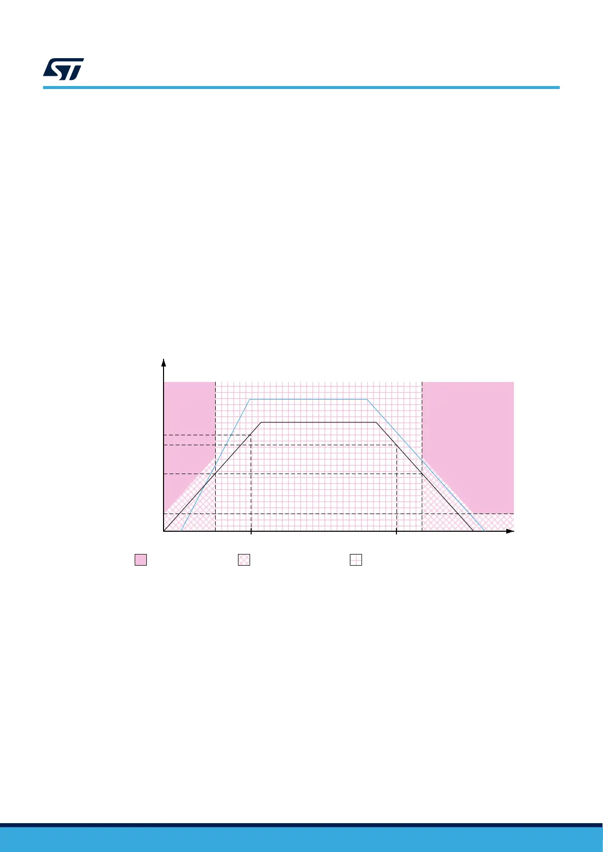
Figure 11. Power-up/power-down sequence
DT47490V2
0.3
1
V
PDR
3.6
Operating modePower-on Power-down time
V
V
DDX
(1)
V
DD
Invalid supply area V
DDX
< V
DD
+ 300 mV
V
DDX
independent from V
DD
V
POR
(1) V
DDX
refers to any power supply among V
DDA
, V
DDUSB
, and V
DDIO2
.
Note: V
BAT
is an independent supply and has no constraint versus V
DD
. All power supply rails can be tied together.
2.3.3 Particular conditions during the power-down phase
During the power-down phase, V
DD
can temporarily become lower than other supplies only if the energy provided
to the MCU remains below 1 mJ. This allows external decoupling capacitors to be discharged with different time
constants during the power-down transient phase (see Figure 11).
V
DDX
(V
DDA
, V
DDIO2
, or V
DDUSB
) power rails must be switched off before V
DD
.
Note: During the power-down transient phase, V
DDX
can remain temporarily above V
DD
(see Figure 11).
AN5373
Power supply sequence between VDDA, VDDUSB, VDDIO2, and VDD
AN5373 - Rev 6
page 18/47

 Loading...


