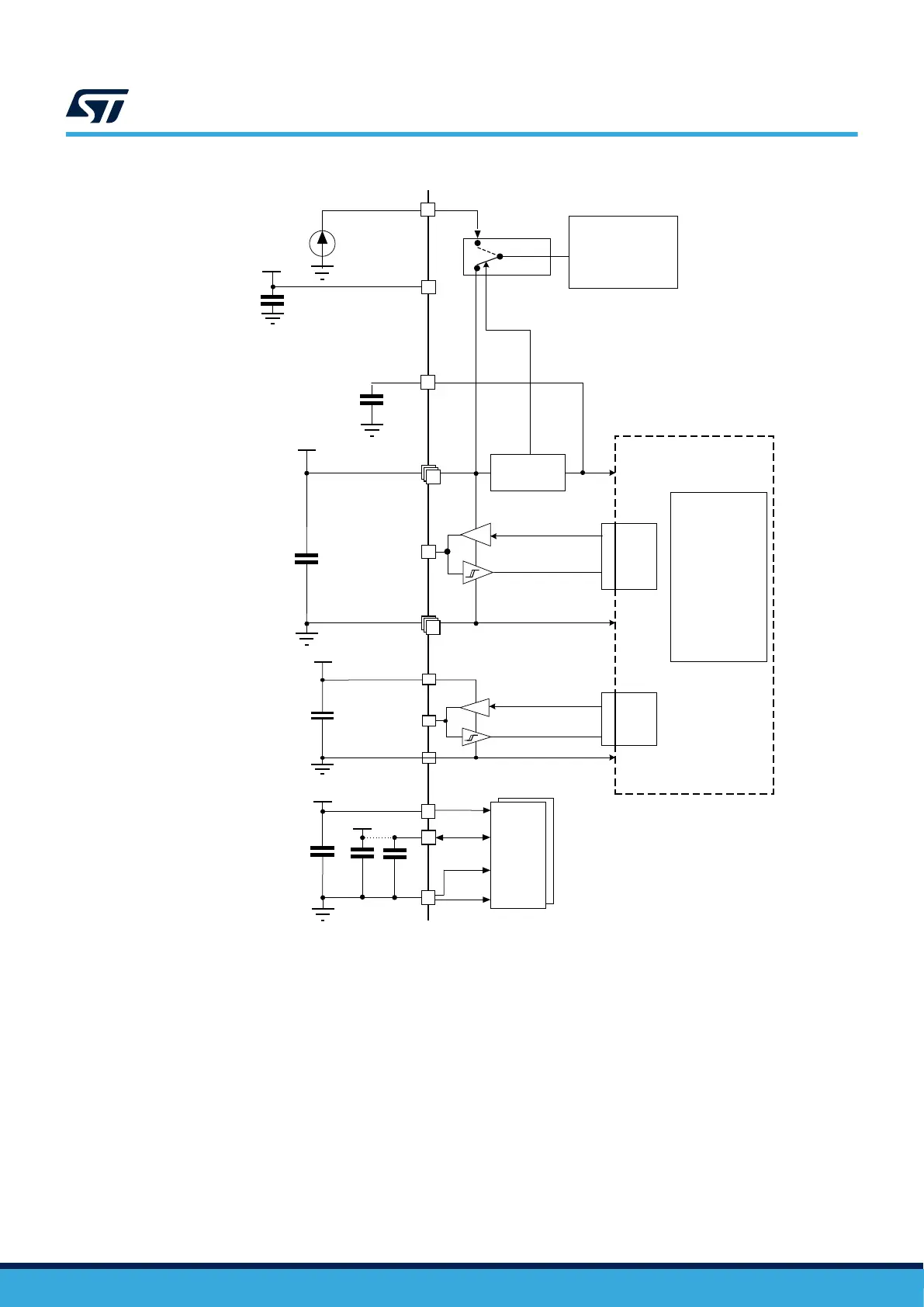
Figure 10. Power supply scheme for STM32U5F/5G/59/5Axxx (without SMPS)
DT71165V1
V
DDIO2
V
DD
Kernel logic
(CPU, digital
and memories)
Level shifter
I/O
logic
Backup circuitry
(LSE, RTC, TAMP,
backup registers,
backup SRAM)
IN
OUT
GPIOs
1.65 – 3.6 V
IN
OUT
GPIOs
m x100 nF
Level shifter
I/O
logic
+ 4.7 µF
m x VDDIO2
m x VSS
n x VSS
n x VDD
VBAT
V
CORE
Power switch
V
DDIO2
V
DDIO1
ADCs/
DACs/
OPAMPs/
COMPs/
VREFBUF
VREF+
VREF-
V
DDA
100 nF
+ 1 µF
VDDA
VSSA
V
REF
100 nF
+ 1 µF
VCAP
4.7 µF
VDDUSB
V
DDUSB
100 nF
LDO
regulator
V
CORE
Note: • SMPS and LDO regulators provide, in a concurrent way, the V
CORE
supply depending on application
requirements. However, only one of them is active at the same time. When SMPS is active, it feeds the
V
CORE
on the two VDD11 pins provided through the SMPS VLXSMPS output pin. A 2.2 µH coil and a
2.2 μF capacitor on each VDD11 pin are then required. When LDO is active, it provides the V
CORE
and
regulates it using the same decoupling capacitors on VDD11 pins.
• It is recommended to add a decoupling capacitor of 100 nF near each VDD11 pin/ball, but it is not
mandatory.
AN5373
Power supply schemes
AN5373 - Rev 6
page 17/47
 Loading...


