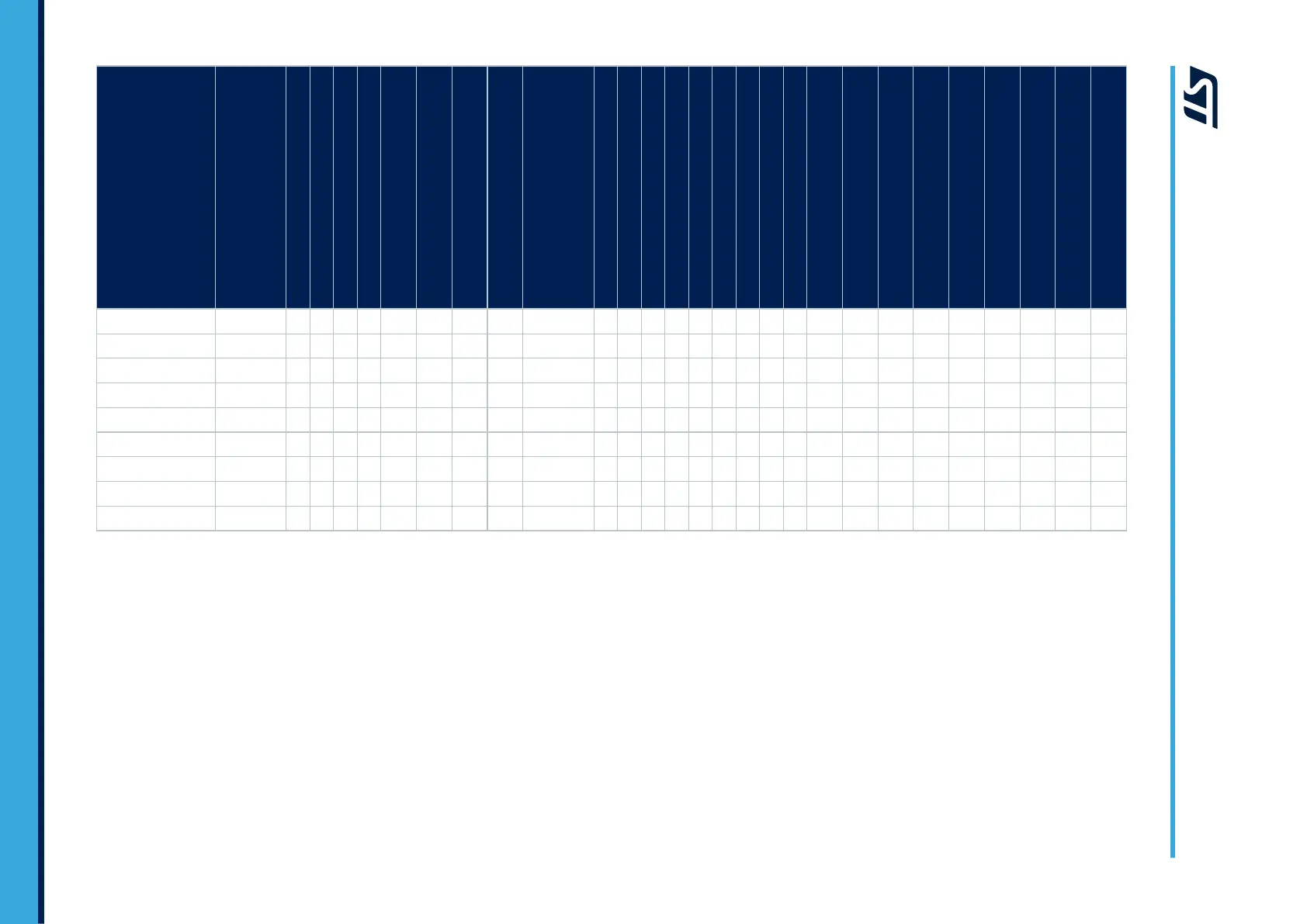
Pin name
LQFP48
UFQFPN48
LQFP64
UFBGA64
LQFP100
UFBGA100
UFBGA132
LQFP144
UFBGA169
TFBGA169
LQFP48 SMPS
UFQFPN48 SMPS
WLCSP56 SMPS
LQFP64 SMPS
UFBGA64 SMPS
WLCSP72 SMPS
WLCSP90 SMPS
LQFP100 SMPS
LQFP100 DSI SMPS
UFBGA100 SMPS
UFBGA132 SMPS
LQFP144 SMPS
LQFP144 DSI SMPS
UFBGA144 DSI SMPS
WLCSP150 SMPS
WLCSP150 DSI SMPS
UFBGA169 SMPS
TFBGA169 SMPS
WLCSP208 DSI SMPS
TFBGA216 DSI SMPS
VSSSMPS - - - - - - - - - X X X X X X X X X X X X X X X X X X X
VLXSMPS - - - - - - - - - X X X X X X X X X X X X X X X X X X X
VCAP X X X X X X X X X - - - - - - - - - - - - - - - - - - -
VDDDSI - - - - - - - - - - - - - - - - X - - - X X - X - - X X
VDD11DSI - - - - - - - - - - - - - - - - X - - - X X - X - - X X
VSSDSI - - - - - - - - - - - - - - - - X - - - X X - X - - X X
VDD11USB - - - - - - - - - - - - - - - - - - - - - - - X - - X X
Number of VDD 3 3 3 5 5 6 9 10 10 3 3 3 4 4 4 5 9 5 6 9 10 8 9 9 10 10 17 10
Number of VSS 3 4 4 5 5 6 11 11 11 3 4 3 3 6 4 5 7 6 6 11 10 12 12 10 11 11 19 20
1. 'X' means that the pin is present.
2. 'o' means that VDD and VDDUSB are internally connected and available on a single pin.
3. 'o' means that VSSA and VREF- are internally connected and available on a single pin.
4. 'o' means that VDDA and VREF+ are internally connected and available on a single pin.
5. '-' means that the pin is absent.
Caution: Packages with and without SMPS are not compatible, in almost all power supply pins of Table 2.
Example: VDDIO2 is the pin number 130 on SMPS package. Pin 130 on the package without SMPS is mapped to a VSS pin. It means that the system
is short‑circuited when a legacy package is mounted on an SMPS socket.
AN5373
- Rev 6
page 24/47
AN5373
Pinout summary
 Loading...


