MCU
function
STM32
pin
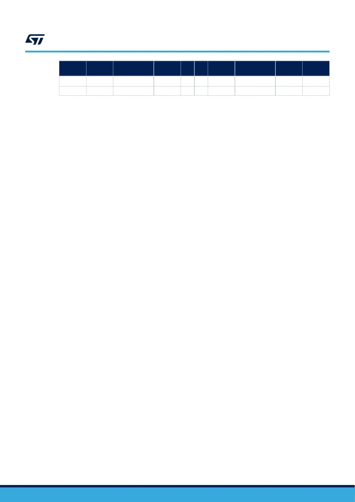
Signal name Pin name Pin Pin Pin name Signal name
STM32
pin
MCU
function
TIM1_CH1 PA8 TIM_D_PWM1 D33 31 32
D36
(4)
TIM_C_PWM2 PB10 TIM2_CH3
TIM4_ETR PE0 TIM_B_ETR D34 33 34 D35 TIM_C_PWM3 PB11 TIM2_CH4
1. The default configuration for the D0/D1 signal is LPUART1 on PG7 and PG8, USART1 on PA9 and PA10 is connected by
default on STLINK-V3E.
2. PG2 to PG15 can have a different I/O level to other I/Os because supplied by VDDIO.
3. I/O shared between ADC and QSPI (exclusive)
4. I/O shared between QSPI and motor control (exclusive)
5. I/O shared between SAI_D, SPI_B, and UCPD function (exclusive)
6. I/Os are shared between SAI and JTAG SWO (exclusive)
7. SAI_D and SAI_B groups are on the same SAI instance (exclusive).
8. SAI_D group is shared with SPI_B group, (exclusive).
UM2861
Zio connectors supporting ARDUINO® Uno V3
UM2861 - Rev 2
page 35/49