2-20
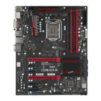
SUPER P4DC6/P4DC6+/P4DC6+II/P4DCE/P4DCE+/P4DCE+II User's Manual
IDE Connectors
There are no jumpers to config-
ure the onboard IDE interfaces
J6 and J7. Refer to Table 2-36
for pin definitions. You must
use the ATA100/66 cable in-
cluded with your system to ben-
efit from the ATA100/66 technol-
ogy.
Floppy Connector
The floppy connector is designated
as JP5. See Table 2-35 for pin
definitions.
Pin Number Function
1 GND
3 GND
5 Key
7 GND
9 GND
11 GND
13 GND
15 GND
17 GND
19 GND
21 GND
23 GND
25 GND
27 GND
29 GND
31 GND
33 GND
Pin Number Function
2 FDHDIN
4 Reserved
6 FDEDIN
8
Index-
10 Motor Enable
12 Drive Select B-
14 Drive Select A-
16 Motor Enable
18 DIR-
20 STEP-
22 Write Data-
24 Write Gate-
26 Track 00-
28 Write Protect-
30 Read Data-
32 Side 1 Select-
34 Diskette
Table 2-35
Floppy Connector Pin Definitions (JP5)
Pin Number Function
1 Reset IDE
3 Host Data 7
5 Host Data 6
7 Host Data 5
9 Host Data 4
11 Host Data 3
13 Host Data 2
15 Host Data 1
17 Host Data 0
19 GND
21 DRQ3
23 I/O W rite-
25 I/O Read-
27 IOCHRDY
29 DACK3-
31 IRQ14
33 Addr 1
35 Addr 0
37 Chip Select 0
39 Activity
Pin Number Function
2 GND
4 Host Data 8
6 Host Data 9
8 Host Data 10
10 Host Data 11
12 Host Data 12
14 Host Data 13
16 Host Data 14
18 Host Data 15
20 Key
22 GND
24 GND
26 GND
28 BALE
30 GND
32 IOCS16-
34 GND
36 Addr 2
38 Chip Select 1-
40 GND
Table 2-36
IDE Connector Pin Definitions (J6, J7)