2-12
SUPER P4DC6/P4DC6+/P4DC6+II/P4DCE/P4DCE+/P4DCE+II User's Manual
Pin
Number
1
2
3
Definition
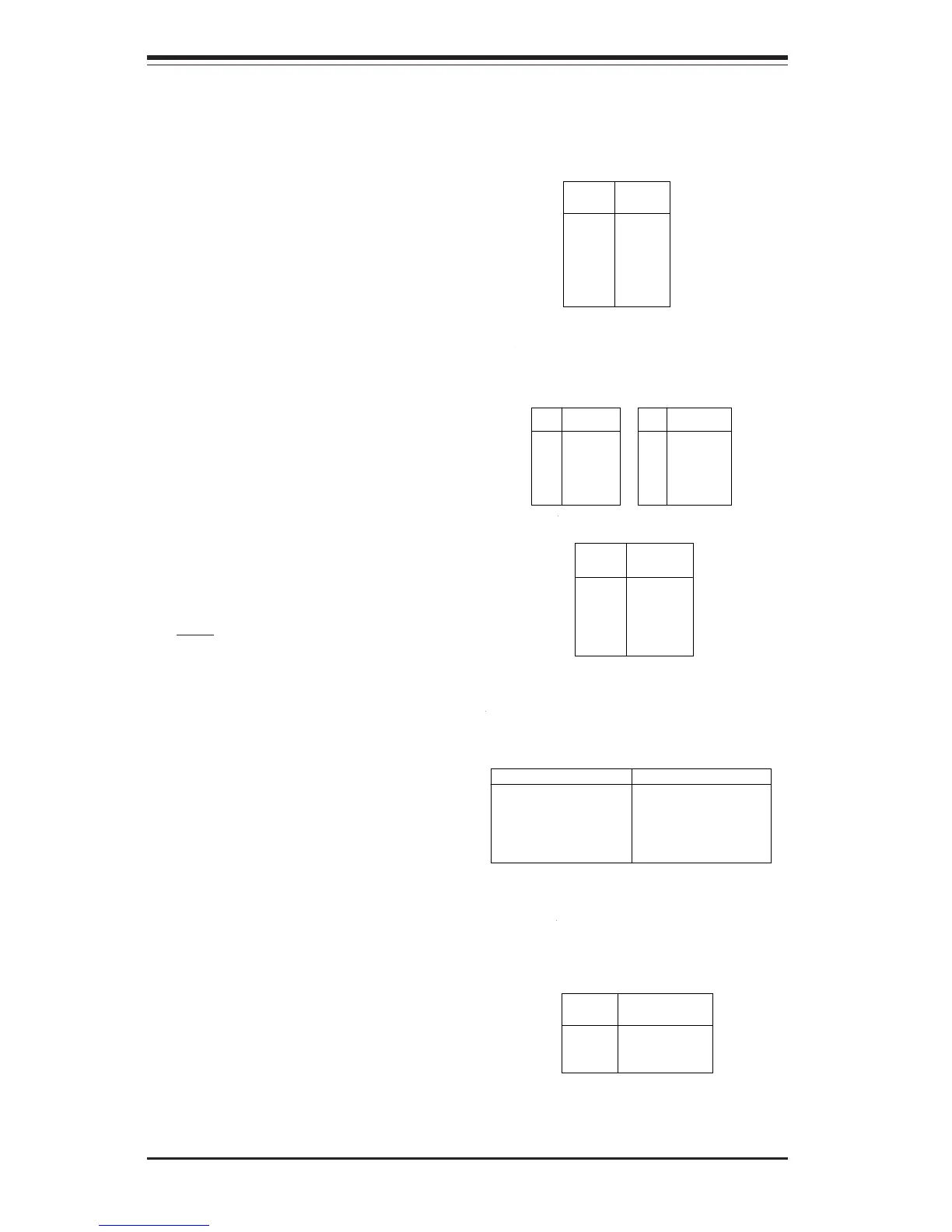
+5v Standby
Ground
Wake-up
Table 2-19
Wake-On-LAN Pin
Definitions (WOL)
Wake-On-LAN
The Wake-On-LAN header is
marked WOL. Refer to Table 2-19
for pin definitions. You must en-
able the LAN Wake-Up setting in
BIOS to use this function. (You
must also have a LAN card with a
Wake-on-LAN connector and cable
to use this feature.)
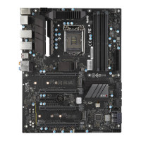
Universal Serial Bus
(USB)
Two Universal Serial Bus connec-
tors (USB0 and USB1) are located
at J18 and J19. See Table 2-17 for
pin definitions. Your motherboard
also provides support for two addi-
tional USB ports: the USB2 (J20)
and USB3 (J29) headers are lo-
cated near the CNR slot.
Note: If you have the USB on JF1
connected you cannot use USB2.
Table 2-17
Universal Serial Bus Pin Definitions
Pin# Definition
1 +5v
2 P0-
3 P0+
4 Ground
Pin# Definition
1 +5v
2 P0-
3 P0+
4 Ground
J18
J19
Serial Ports
Two serial connectors are
provided on your board: COM1
(J16) and COM2 (J22). See
Table 2-18 for pin definitions.
ATX PS/2 Keyboard and
PS/2 Mouse Ports
The ATX PS/2 keyboard and the
PS/2 mouse are located at J17.
See Table 2-16 for pin definitions.
(The mouse port is above the key-
board port. See Figure 2-4 for lo-
cations.)
Table 2-16
PS/2 Keyboard
and Mouse Port
Pin Definitions
(J17)
Pin
Number
1
2
3
4
5
6
Definition
Data
NC
Ground
VCC
Clock
NC
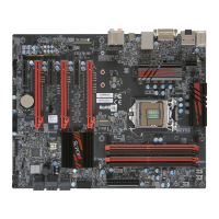
(USB 2-J20 & USB3-J29)
Pin
Number
1
2
3
4
5
Definition
+5V
PO-
PO+
Ground
Ground
Table 2-18
Serial Port Pin Definitions COM1-J16 &
COM2-J22
Pin Number Definition
1 CD
2 RD
3 TD
4 DTR
5 Ground
Pin Number Definition
6 DSR
7 RTS
8 CTS
9 RI
10 NC
Note: Pin 10 is included on the header but not on
the port.