1-8
SUPER P4DC6/P4DC6+/P4DC6+II/P4DCE/P4DCE+/P4DCE+II User’s Manual
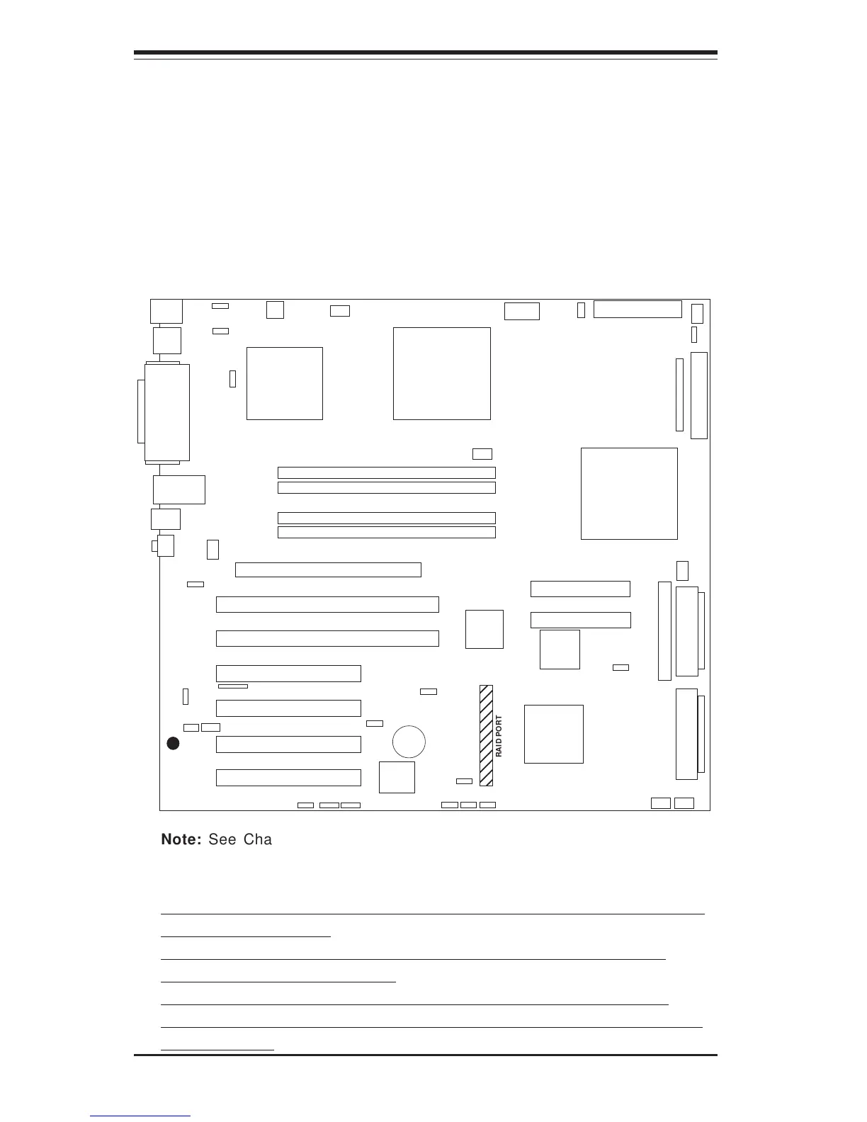
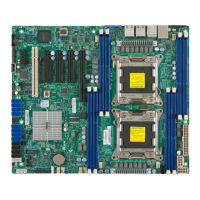
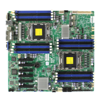
Figure 1-4. SUPER P4DC6+/P4DCE+ Layout
(not drawn to scale)
SUPER P4DC6+
KB/
MOUSE
USB0,1
PARALLEL
PORT
COM 1
COM 2
MCH
LAN
LINE OUT/
LINE IN
MIC
J17
J18/
J19
J16
J15
J22
J27
J31
J30
J23
CPU #2
CPU #1
ATX POWER
JPWAKE
CPU FAN2
4-PIN
12vDC
8-PIN
12vDC
J24
CH FAN4
JF1
FLOPPY
CPU FAN1
PWR
FAULT
RAMBUS CHB BANK 0
RAMBUS CHA BANK 1
RAMBUS CHB BANK 1
RAMBUS CHA BANK 0
PCI 4
PCI 3
PCI-64 #1
AGP PRO
PCI-64 #2
PCI 1
PCI 2
CD 1
CD 2
IDE #1
IDE #2
J7
J6
P64H
ICH2
AIC-7899
CH FAN3
ULTRA SCSI CH B
ULTRA III LVD/SE
SCSI CH B
ULTRA III LVD/SE
SCSI CH A
JA2
JA3
JA1
BIOS
BATTERY
J20JP4
J29
JWOR JPA1
JPA2
CH
FAN1
CH
FAN2
JBT1
OH FAN
JOH
JP35
J32
WOL
JP34
JP38
JP37
JP36
JP39
JP5
RAID PORT
Note: See Chapter 2 for more information on jumper settings and pin
definitions. On a 2-pin jumper, "Closed" means the jumper is on both pins
and "Open" means the jumper is either off or on one pin only.
The P4DCE+ shares the same layout as the P4DC6+ but with no onboard
SCSI and no RAID port.
The P4DC6+II shares the same layout as the P4DC6+ but includes a
heatsink over the VRM modules.
The P4DCE+II shares the same llayout as the P4DCE+ but includes a
heatsink over the VRM modules. Both "II" models support processors of
up to 2.80 GHz.
JPA3