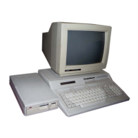
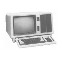
Tandy 1000
8259AJ8259A-~8259A-8
Technical Reference Manual
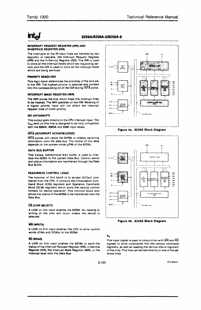
Figure 4a. 8259A
Block
Diagram
INTERRUPT REQUEST REGISTER (IRR) AND
IN·SERVICE REGISTER (ISR)
The
interrupts
at the IR Input lines are handled by
two
registers in cascade, the Interrupt Request Register
(IRR) and the In-Service Register (ISR). The IRR is used
to
store all
the
interrupt
levels which are requesting ser·
vice; and the ISR is used
to
store all the
interrupt
levels
which
are being serviced.
PRIORITY RESOLVER
This
logic
block
determines
the
priorities
01
the
bits
set
in the IRA. The highest
priority
is selected and strobed
into
the corresponding bit
01
the ISR during INTA pulse.
INTERRUPT MASK REGISTER (IMR)
The IMR
stores
the
bits
which mask
the
interrupt
lines
to
be masked. The IMR operates on the IRA. Masking
of
a
higher
priority
input
will
not
affect
the interrupt
request lines
of
lower priority.
INT (INTERRUpn
This
output
goes
directly
to
the
CPU
interrupt
input. The
V
OH
level on
this
line
is
designed
to
be
lully
compatible
with
the
808OA,
BOS5A
and 8086
input
levels.
INTA (INTERRUPT ACKNOWLEDGE)
INTA pulses
will
cause the 8259A
to
release vectoring
information
onto
the data bus. The
lormat
of
this
data
depends on the
system
mode ("PM)
of
the 8259A.
DATA BUS BUFFER
This 3-state,
bidirectional
8-bit
buffer
is used
to
inter-
lace the 8259A
to
the
system
Data Bus. Control words
and status
information
are translerred through the Dafa
Bus Buller.
READIWRITE CONTROL LOGIC
The
lunction
01
this
block
is
to
accept OUTput com-
mands
Irom
the CPU. It contains the Initialization Com-
mand Word (ICW) regisfers and Operation Command
Word (OCW) registers which store the various
control
lormats
lor
device operation. This
function
block
also
allows the status
of
the 8259A to be translerred
onto
the
Data Bus.
CS
(CHIP
SELECn
A LOW on
this
input
enables the 8259A. No reading
or
writing
of
the
chip
will
occur
unless the device is
selected.
"'~
___
<I(AO'
-o-
R
,",,==f;l-
'""-y
9IiN
_
'""~
C"'S I
llU"fJl.
~
(A$1
g.'iN_~
__
~
I
WR(WRITE)
A LOW on
this
input
enables the
CPU
to
write
control
words (ICWs and
OCWS)
to
the 8259A.
AD
(READ)
A LOW on
this
input
enables the 8259A to send the
status
01
the Interrupt Request Register
(IRR),
In Service
Register (ISR),
the
Interrupt Mask Register (IMR), or the
Interrupt level
onto
the Data Bus.
2-123
Figure 4b. 8259A
Block
Diagram
A
o
This
input
signal
is
used in
conjunction
with
WA
and
AD
signals
to
write
commands
into
the
various command
registers, as well as reading the various status registers
of
the
chip. This
line
can
be
tied
directly
to one
of
the
ad-
dress lines.
AFN·OO221E
 Loading...