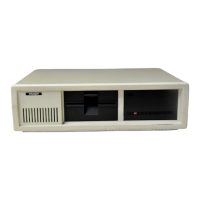
Tandy 1000
Technical Reference Manual
inter
8284A/8284A-1
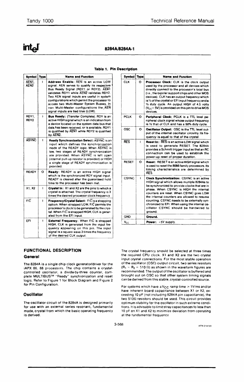
Table
1.
Pin Description
Symbol
Type
Nama
and
FuncUon
ClK
0 Proceaeor
Clock:
ClK
is the clock
output
used by the processor and all devices which
directly
connect
to the processor's local bus
(i.e., the
bipolar
support chips and other MOS
devices).
ClK
has an
output
frequency which
is
Y3
of
the
crystal
or
EFI
input
frequency anda
I
r~c:~~~~~I:~O~~d::Ut~i~I~~
t~~~~~
~~~
devices.
PClK
0
Peripheral
Clock:
PCLK is a
TIL
level pe-
ripheral
clock
signal whose
output
frequency
~
is
'12
that
of
ClK
and has a
50%
duty cycle.
OSC
0
Oecllla'or
Output:
OSC is the
TIL
level out-
put
of
the
internal oscillator circuitry. Its fr&-
quency
is
equal
to
that
of
the crystal.
RES
I
Reaet
In:
RES
is an active
lOW
signal which
is
used
to
generate
RESET. The 8284A
provides a Schmin
trigger
input
so that
an
RC
connection
can
be
used
to
establislol the
power-up reset
of
proper
duration.
RESET
0 Reaet: RESET
is
an active HIGH signal which
is used
to
reset the 8086 family processors. Its
timing
characteristics
are determined by
RES.
CSYNC I
Clock
SynchronIzation:
CSYNC is
an
'active
HIGH
signal which allows multiple 8284As to
be
synchronized to provide clocks that are in
phase. When CSYNC is HIGH the internal
counters are reset. When CSYNC goes
lOW
the internal counters are allowed to resume
counting. CSYNC needs to
be
externally syn-
chronized
to
Eft.
When using the internal os-
cillator
CSYNC
should
be
hardwired
to
ground.
GND
Ground.
, V
cc
Power: +5V supply
Name and
Function
Cryatalln:
Xl
and
X2
are the pins to which a
crystal is anached. The crystal frequency
is
3
times the desired processor clock frequency.
Frequency/Crya'a' Select:
FIC
is astrapping
option. When strapped
lOW,
FIG
permits the
processor's clock to
be
generated
by
the crys-
tal. When
FIGis strapped HIGH,
ClK
is gener-
ated from the
EFI
input.
Ready Synchronization
Select:
ASYNC
is
an
input
which
defines
the
synchronization
mode
of
the READY logic. When ASYNC
is
low,
two
stages
of
READY synchronization
are
provided.
When ASYNC is
left
open
(internal pull-up resistor
is
provided) or
HIGH
a single stage of READY synchronization
is
provided.
Addre
••
Enable:
AEN is an active
lOW
signal.
AEN
serves to qualify its respective
Bus Ready Signal (RDYl
or
RDY2). AENl
validates RDYl while AEN2 validates
RDY2.
Two
AEN
signal inputs are useful in system
configurations which permit the processor to
access
two
Multi-Master System Busses. In
non
Multi-Master
configurations
the,AEN
signal inputs are tied true (lOW).
Bua Ready: (Transfer Complete).
ROY
is
an
active HIGH signal which
is
an
indicationfrom
a device located on the system data bus that
data has been received,
or
is available. RDYl
is qualified by AENl while
RDY2
is qualified
by AEN2.
o
Ready:
READY is
an
active HIGH
signal
which is the synchronized
ROY
signal input
READY is cleared
aller
the guaranteed hold
time to the processor has been met.
Xl,
X2
EFI
ASYNC
FIC
RDY1,
RDY2
READY
Symbol Type
AEN1,
AEN2
External Frequency: When
FIC
is
strapped
HIGH.
ClK
is generated from the Input
fr&-
quency
appearing
on this pin. The
input
signal is a square wave 3 times the frequency
'--_-----'_.----'-_of_t_he_d_e_si_re_d_C_l_K_o_ut-'-pu_t_.
-------
FUNCTIONAL DESCRIPTION
General
The
8284A
is
a
single
Chip
clock
generator/driver
for
the
iAPX
86,
88
processors.
The
chip
contains
a
crystal-
controlled
oscillator,
a
divide-by-three
counter,
com-
plete
MUlTIBUSTM
"Ready"
synchronization
and
reset
logic.
Refer
to
Figure
1
for
Block
Diagram
and
Figure
2
for
Pin
Configuration.
Oscillator
The
oscillator
circuit
of
the
8284A
is
designed
primarily
for
use
with
an
external
series
resonant,
fundamental
mode,
crystal
from
which
the
basic
operating
frequency
is
derived.
The
crystal
frequency
should
be
selected
at
three
times
the
required
CPU
clock.
Xl
and
X2
are
the
two
crystal
input
crystal
connections.
For
the
most
stable
operation
of
the
oscillator
(OSC)
output
circuit,
two
series
resistors
(R,
= R
2
=
510
fl)
as
shown
in
the
waveform figures
are
recommended.
The
output
of
the
oscillator
is
buffered
and
brought
out
on
OSC
so
that
other
system
timing
signals
can
be
derived
from
this
stable,
crystal-controlled
source.
For
systems
which
have
a VCC
ramp
time""
1
Vlms
andlor
have
inherent
board
capacitance
between
Xl
or
X2, ex-
ceeding
10
pF
(not
including
8284A
pin
capacitance).
the
two
S10n
resistors
should
be
used.
This
circuit
provides
optimum
stability
for
the
oscillator
in
such
extreme
condi-
tions.
It
is
advisable
to
limit
stray
capacitances
to
les$
than
10 pF
on
Xl
and
X2
to
minimize
deviation
from
operating
at
the
fundamental
frequencv
3-568
AFN-OU72D
 Loading...