MSP430F5529
,
MSP430F5528
,
MSP430F5527
,
MSP430F5526
MSP430F5525
,
MSP430F5524
,
MSP430F5522
,
MSP430F5521
MSP430F5519, MSP430F5517, MSP430F5515, MSP430F5514, MSP430F5513
SLAS590M –MARCH 2009–REVISED NOVEMBER 2015
www.ti.com
6.9.11 TA0 (Link to User's Guide)
TA0 is a 16-bit timer and counter (Timer_A type) with five capture/compare registers. It can support
multiple capture/compare registers, PWM outputs, and interval timing. It also has extensive interrupt
capabilities. Interrupts may be generated from the counter on overflow conditions and from each of the
capture/compare registers.
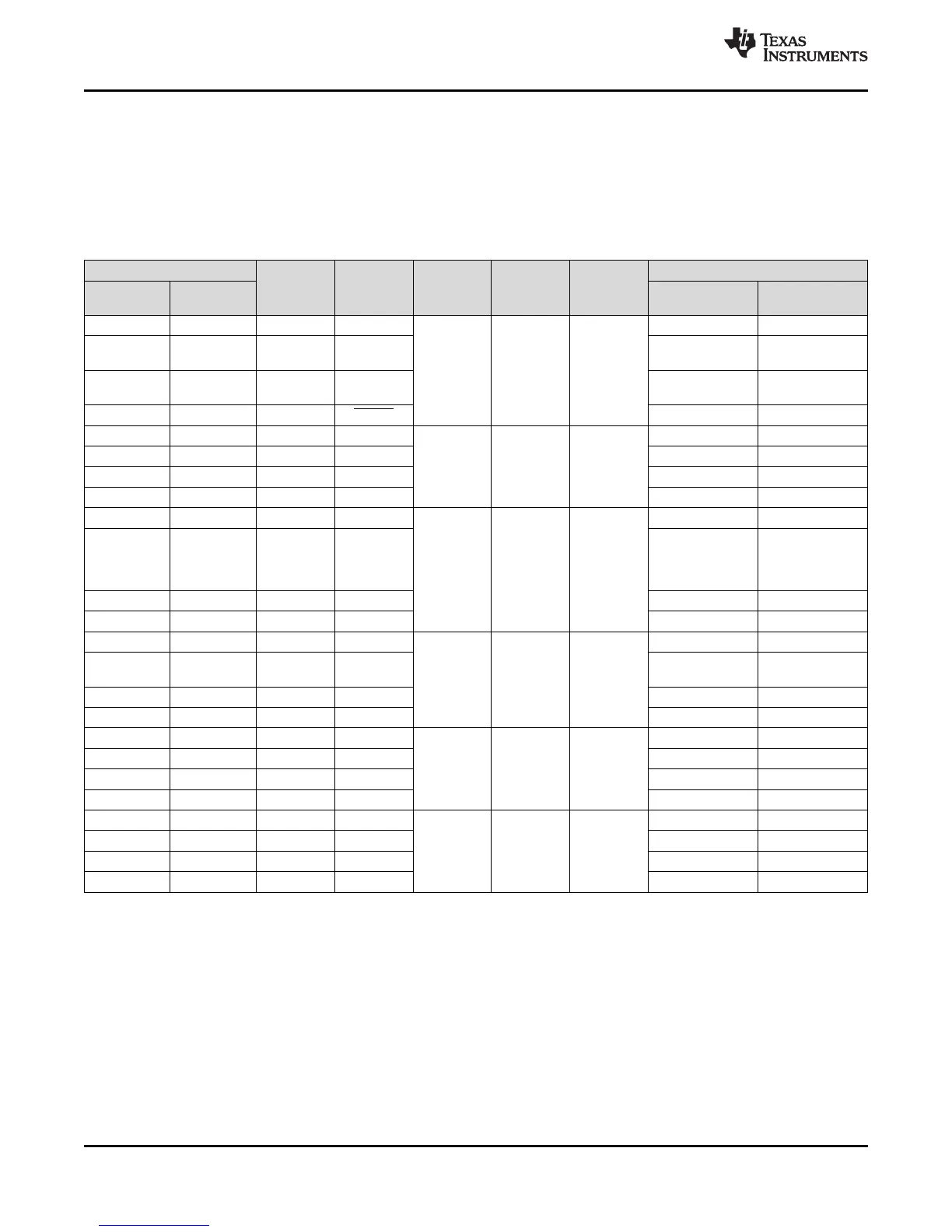
Table 6-11. TA0 Signal Connections
INPUT PIN NUMBER OUTPUT PIN NUMBER
DEVICE MODULE MODULE DEVICE
MODULE
INPUT INPUT OUTPUT OUTPUT
RGC, YFF,
BLOCK
PN RGC, YFF, ZQE PN
SIGNAL SIGNAL SIGNAL SIGNAL
ZQE
18, H2-P1.0 21-P1.0 TA0CLK TACLK
ACLK
ACLK
(internal)
Timer NA NA
SMCLK
SMCLK
(internal)
18, H2-P1.0 21-P1.0 TA0CLK TACLK
19, H3-P1.1 22-P1.1 TA0.0 CCI0A 19, H3-P1.1 22-P1.1
DV
SS
CCI0B
CCR0 TA0 TA0.0
DV
SS
GND
DV
CC
V
CC
20, J3-P1.2 23-P1.2 TA0.1 CCI1A 20, J3-P1.2 23-P1.2
ADC12 ADC12
CBOUT (internal)
(1)
(internal)
(1)
CCI1B
(internal) ADC12SHSx = ADC12SHSx =
CCR1 TA1 TA0.1
{1} {1}
DV
SS
GND
DV
CC
V
CC
21, G4-P1.3 24-P1.3 TA0.2 CCI2A 21, G4-P1.3 24-P1.3
ACLK
CCI2B
(internal)
CCR2 TA2 TA0.2
DV
SS
GND
DV
CC
V
CC
22, H4-P1.4 25-P1.4 TA0.3 CCI3A 22, H4-P1.4 25-P1.4
DV
SS
CCI3B
CCR3 TA3 TA0.3
DV
SS
GND
DV
CC
V
CC
23, J4-P1.5 26-P1.5 TA0.4 CCI4A 23, J4-P1.5 26-P1.5
DV
SS
CCI4B
CCR4 TA4 TA0.4
DV
SS
GND
DV
CC
V
CC
(1) Only on devices with ADC.
62 Detailed Description Copyright © 2009–2015, Texas Instruments Incorporated
Submit Documentation Feedback
Product Folder Links: MSP430F5529 MSP430F5528 MSP430F5527 MSP430F5526 MSP430F5525 MSP430F5524
MSP430F5522 MSP430F5521 MSP430F5519 MSP430F5517 MSP430F5515 MSP430F5514 MSP430F5513
 Loading...


