/NR
/1 to /64
OSCIN
PLL
INTCLK
/OD
/1 to /8
VCOCLK
/R
/1 to /32
post_ODCLK
/NF
/1 to /256
PLLCLK
/NR2
/1 to /64
OSCIN
PLL#2
INTCLK2
/OD2
/1 to /8
VCOCLK2
/R2
/1 to /32
post_ODCLK2
/NF2
/1 to /256
PLL2CLK
f
PLLCLK
= (f
OSCIN
/ NR) * NF / (OD * R)
f
PLL2CLK
= (f
OSCIN
/ NR2) * NF2 / (OD2 * R2)
RM46L852
www.ti.com
SPNS185 –SEPTEMBER 2012
4.6.1.3 Phase Locked Loop (PLL) Clock Modules
The PLL is used to multiply the input frequency to some higher frequency.
The main features of the PLL are:
• Frequency modulation can be optionally superimposed on the synthesized frequency of PLL1. The
frequency modulation capability of PLL2 is permanently disabled.
• Configurable frequency multipliers and dividers.
• Built-in PLL Slip monitoring circuit.
• Option to reset the device on a PLL slip detection.
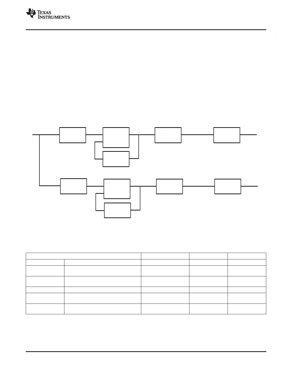
4.6.1.3.1 Block Diagram
Figure 4-6 shows a high-level block diagram of the two PLL macros on this microcontroller. PLLCTL1 and
PLLCTL2 are used to configure the multiplier and dividers for the PLL1. PLLCTL3 is used to configure the
multiplier and dividers for PLL2.
Figure 4-6. PLLx Block Diagram
4.6.1.3.2 PLL Timing Specifications
Table 4-11. PLL Timing Specifications
PARAMETER MIN MAX UNIT
f
INTCLK
PLL1 Reference Clock frequency 1 f
(OSC_SQR)
MHz
f
post_ODCLK
Post-ODCLK – PLL1 Post-divider input 400 MHz
clock frequency
f
VCOCLK
VCOCLK – PLL1 Output Divider (OD) input 150 550 MHz
clock frequency
f
INTCLK2
PLL2 Reference Clock frequency 1 f
(OSC_SQR)
MHz
f
post_ODCLK2
Post-ODCLK – PLL2 Post-divider input 400 MHz
clock frequency
f
VCOCLK2
VCOCLK – PLL2 Output Divider (OD) input 150 550 MHz
clock frequency
Copyright © 2012, Texas Instruments Incorporated System Information and Electrical Specifications 65
Submit Documentation Feedback