RM46L852
SPNS185 –SEPTEMBER 2012
www.ti.com
4.6.1.4 External Clock Inputs
The device supports up to two external clock inputs. This clock input must be a square wave input. The
electrical and timing requirements for these clock inputs are specified below.
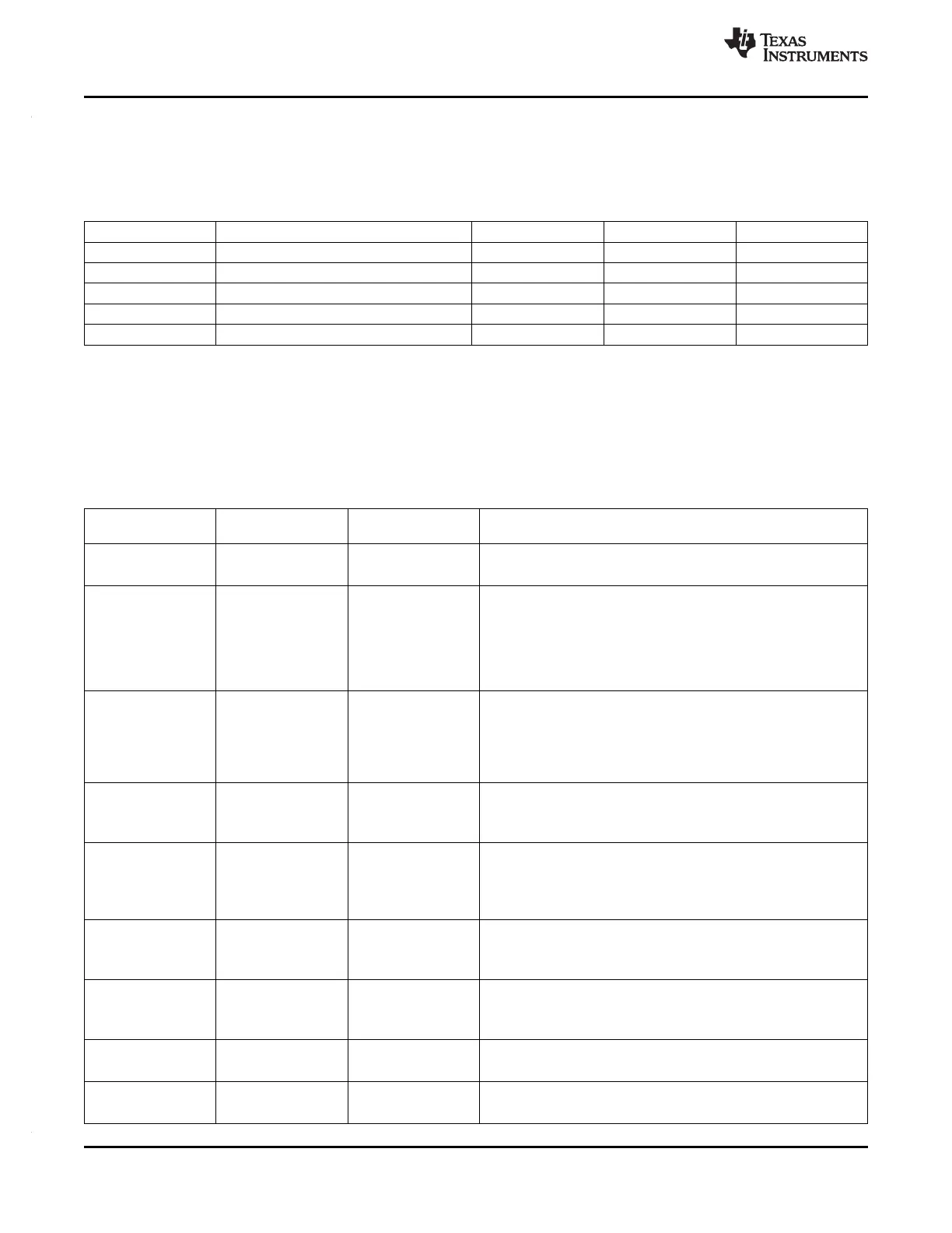
Table 4-12. External Clock Timing and Electrical Specifications
Parameter Description Min Max Unit
f
EXTCLKx
External clock input frequency 80 MHz
t
w(EXTCLKIN)H
EXTCLK high-pulse duration 6 ns
t
w(EXTCLKIN)L
EXTCLK low-pulse duration 6 ns
v
iL(EXTCLKIN)
Low-level input voltage -0.3 0.8 V
v
iH(EXTCLKIN)
High-level input voltage 2 VCCIO + 0.3 V
4.6.2 Clock Domains
4.6.2.1 Clock Domain Descriptions
The table below lists the device clock domains and their default clock sources. The table also shows the
system module control register that is used to select an available clock source for each clock domain.
Table 4-13. Clock Domain Descriptions
Clock Domain Name Default Clock Clock Source Description
Source Selection Register
HCLK OSCIN GHVSRC
• Is disabled via the CDDISx registers bit 1
• Used for all system modules including DMA, ESM
GCLK OSCIN GHVSRC
• Always the same frequency as HCLK
• In phase with HCLK
• Is disabled separately from HCLK via the CDDISx registers bit 0
• Can be divided by 1up to 8 when running CPU self-test (LBIST)
using the CLKDIV field of the STCCLKDIV register at address
0xFFFFE108
GCLK2 OSCIN GHVSRC
• Always the same frequency as GCLK
• 2 cycles delayed from GCLK
• Is disabled along with GCLK
• Gets divided by the same divider setting as that for GCLK when
running CPU self-test (LBIST)
VCLK OSCIN GHVSRC
• Divided down from HCLK
• Can be HCLK/1, HCLK/2, ... or HCLK/16
• Is disabled separately from HCLK via the CDDISx registers bit 2
VCLK2 OSCIN GHVSRC
• Divided down from HCLK
• Can be HCLK/1, HCLK/2, ... or HCLK/16
• Frequency must be an integer multiple of VCLK frequency
• Is disabled separately from HCLK via the CDDISx registers bit 3
VCLK3 OSCIN GHVSRC
• Divided down from HCLK
• Can be HCLK/1, HCLK/2, ... or HCLK/16
• Is disabled separately from HCLK via the CDDISx registers bit 8
VCLK4 OSCIN GHVSRC
• Divided down from HCLK
• Can be HCLK/1, HCLK/2, ... or HCLK/16
• Is disabled separately from HCLK via the CDDISx registers bit 9
VCLKA1 VCLK VCLKASRC
• Defaults to VCLK as the source
• Is disabled via the CDDISx registers bit 4
VCLKA2 VCLK VCLKASRC
• Defaults to VCLK as the source
• Is disabled via the CDDISx registers bit 5
66 System Information and Electrical Specifications Copyright © 2012, Texas Instruments Incorporated
Submit Documentation Feedback