RM46L852
www.ti.com
SPNS185 –SEPTEMBER 2012
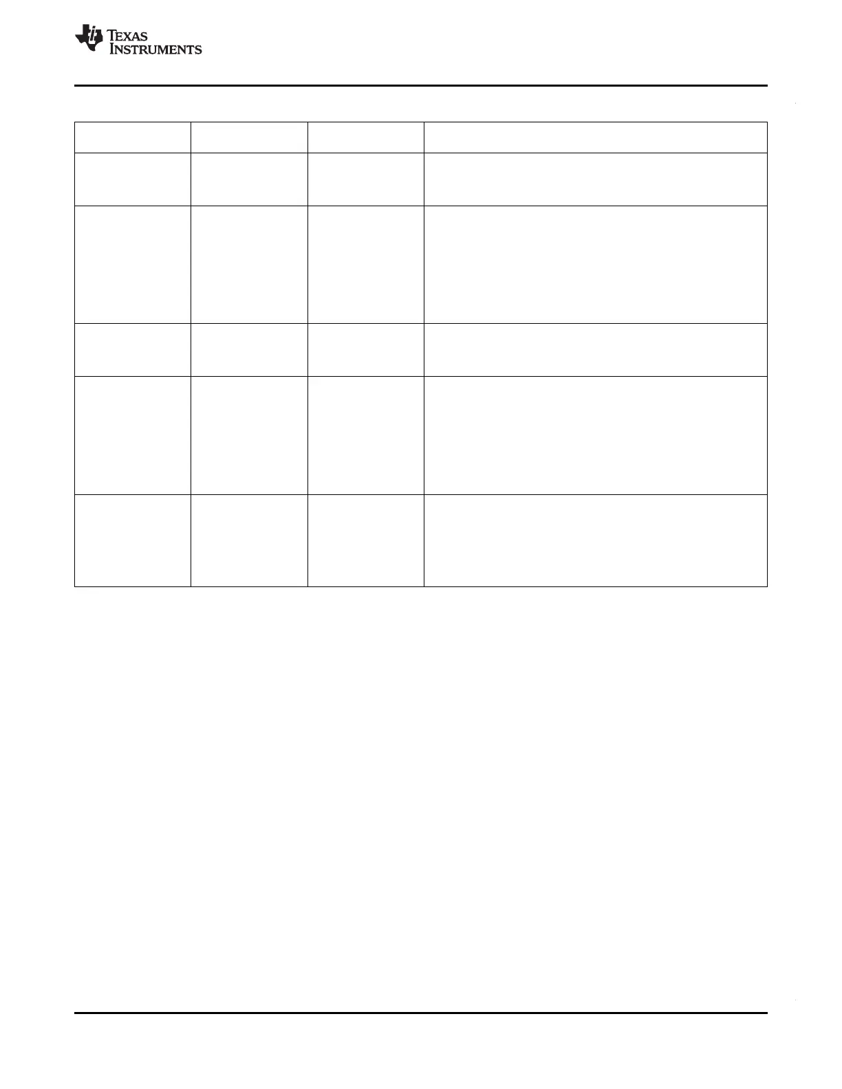
Table 4-13. Clock Domain Descriptions (continued)
Clock Domain Name Default Clock Clock Source Description
Source Selection Register
VCLKA3_S VCLK VCLKACON
• Defaults to VCLK as the source
• Frequency can be as fast as HCLK frequency.
• Is disabled via the CDDISx registers bit 10
VCLKA3_DIVR VCLK VCLKACON1
• Divided down from the AVCLK3_S using the VCLKA3R field of
the VCLKACON1 register at address 0xFFFFE140
• Frequency can be VCLKA3_S/1, VCLKA3_S/2, ..., or
VCLKA3_S/8
• Default frequency is VCLKA3_S/2
• Is disabled separately via the VCLKACON1 register
VCLKA3_DIV_CDDIS bit only if the VCLKA3_S clock is not
disabled
VCLKA4_S VCLK VCLKACON1
• Defaults to VCLK as the source
• Frequency can be as fast as HCLK frequency
• Is disabled via the CDDISx registers bit 11
VCLKA4_DIVR VCLK VCLKACON1
• Divided down from the VCLKA4_S using the VCLKA4R field of
the VCLKACON1 register at address 0xFFFFE140
• Frequency can be VCLKA4_S/1, VCLKA4_S/2, ..., or
VCLKA4_S/8
• Default frequency is VCLKA4_S/2
• Is disabled separately via the VCLKACON1 register
VCLKA4_DIV_CDDIS bit only if the VCLKA4_S clock is not
disabled
RTICLK VCLK RCLKSRC
• Defaults to VCLK as the source
• If a clock source other than VCLK is selected for RTICLK, then
the RTICLK frequency must be less than or equal to VCLK/3
– Application can ensure this by programming the RTI1DIV
field of the RCLKSRC register, if necessary
• Is disabled via the CDDISx registers bit 6
Copyright © 2012, Texas Instruments Incorporated System Information and Electrical Specifications 67
Submit Documentation Feedback