EMA_CLK
EMA_BA[1:0]
EMA_CS[0]
EMA_CAS
EMA_RAS
EMA_WE
CLK
CE
WE
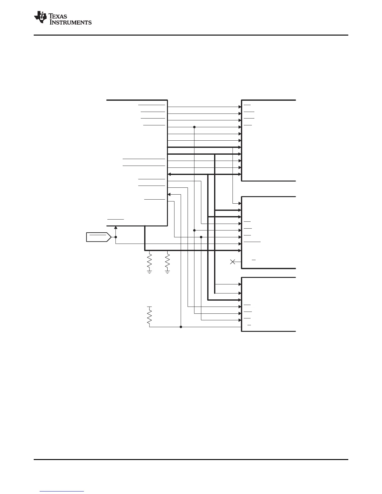
EMIFA
SDRAM
2Mx16x4
Bank
EMA_SDCKE
CAS
RAS
CKE
BA[1:0]
LDQM
UDQM
DQ[15:0]
A[11:0]EMA_A[12:0]
EMA_WE_DQM[0]
EMA_WE_DQM[1]
EMA_D[15:0]
EMA_CS[2]
EMA_CS[3]
EMA_WAIT
EMA_OE
GPIO
(6Pins)
RESET
A[0]
A[12:1]
DQ[15:0]
CE
WE
OE
RESET
A[18:13]
RY/ YB
NOR
FLASH
512Kx16
ALE
CLE
DQ[15:0]
CE
WE
RE
RB
NAND
FLASH
1Gbx16
EMA_BA[1]
EMA_A[1]
EMA_A[2]
...
D
VDD
RESET
109
TMS320C6748
www.ti.com
SPRS590G –JUNE 2009–REVISED JANUARY 2017
Submit Documentation Feedback
Product Folder Links: TMS320C6748
Peripheral Information and Electrical SpecificationsCopyright © 2009–2017, Texas Instruments Incorporated
A likely use case with more than one EMIFA chip select used for NAND flash is illustrated in Figure 6-11.
This figure shows how two multiplane NAND flash devices with two chip selects each would connect to the
EMIFA. In this case if NAND is the boot memory, then the boot image needs to be stored in the NAND
area selected by EMA_CS[3]. Part of the application image could spill over into the NAND regions
selected by other EMIFA chip selects; but would rely on the code stored in the EMA_CS[3] area to
bootload it.
Figure 6-10. Connection Diagram: SDRAM, NOR, NAND