123
TMS320C6748
www.ti.com
SPRS590G –JUNE 2009–REVISED JANUARY 2017
Submit Documentation Feedback
Product Folder Links: TMS320C6748
Peripheral Information and Electrical SpecificationsCopyright © 2009–2017, Texas Instruments Incorporated
(1) Higher DDR2/mDDR speed grades are supported due to inherent JEDEC DDR2/mDDR backwards compatibility.
(2) Supported configurations are one 16-bit DDR2/mDDR memory or two 8-bit DDR2/mDDR memories
6.11.3.2 Compatible JEDEC DDR2/mDDR Devices
Table 6-25 shows the parameters of the JEDEC DDR2/mDDR devices that are compatible with this
interface. Generally, the DDR2/mDDR interface is compatible with x16 DDR2-400/mDDR-200 speed
grade DDR2/mDDR devices.
The device also supports JEDEC DDR2/mDDR x8 devices in the dual chip configuration. In this case, one
chip supplies the upper byte and the second chip supplies the lower byte. Addresses and most control
signals are shared just like regular dual chip memory configurations.
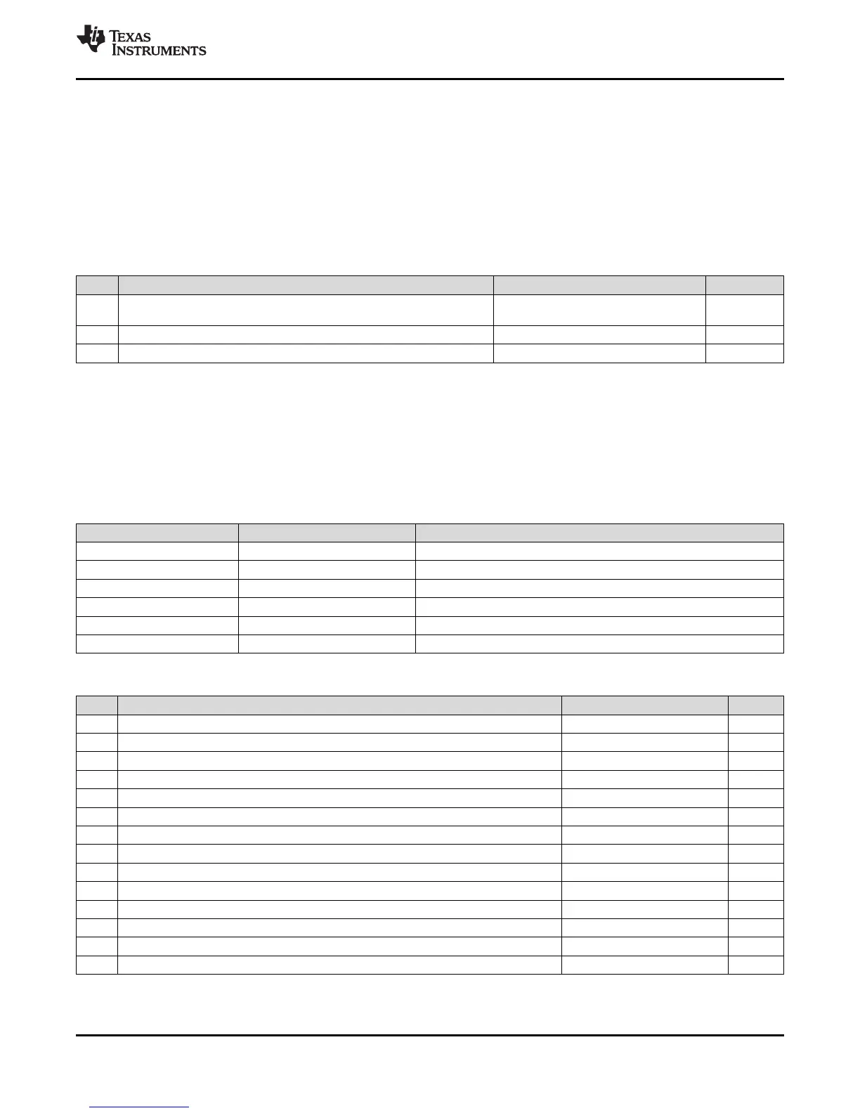
Table 6-25. Compatible JEDEC DDR2/mDDR Devices
NO. PARAMETER MIN MAX UNIT
1 JEDEC DDR2/mDDR Device Speed Grade
(1)
DDR2-400/mDDR-
200
2 JEDEC DDR2/mDDR Device Bit Width x8 x16 Bits
3 JEDEC DDR2/mDDR Device Count
(2)
1 2 Devices
6.11.3.3 PCB Stackup
The minimum stackup required for routing the device is a six layer stack as shown in Table 6-26.
Additional layers may be added to the PCB stack up to accommodate other circuitry or to reduce the size
of the PCB footprint.Complete stack up specifications are provided in Table 6-27 .
Table 6-26. Device Minimum PCB Stack Up
LAYER TYPE DESCRIPTION
1 Signal Top Routing Mostly Horizontal
2 Plane Ground
3 Plane Power
4 Signal Internal Routing
5 Plane Ground
6 Signal Bottom Routing Mostly Vertical
(1) Please refer to the Flip Chip Ball Grid Array Package Reference Guide (SPRU811) for device BGA pad size.
(2) Please refer to the DDR2/mDDR device manufacturer documentation for the DDR2/mDDR device BGA pad size.
(3) Z is the nominal singled ended impedance selected for the PCB specified by item 12.
Table 6-27. PCB Stack Up Specifications
NO. PARAMETER MIN TYP MAX UNIT
1 PCB Routing/Plane Layers 6
2 Signal Routing Layers 3
3 Full ground layers under DDR2/mDDR routing region 2
4 Number of ground plane cuts allowed within DDR routing region 0
5 Number of ground reference planes required for each DDR2/mDDR routing layer 1
6 Number of layers between DDR2/mDDR routing layer and reference ground plane 0
7 PCB Routing Feature Size 4 Mils
8 PCB Trace Width w 4 Mils
8 PCB BGA escape via pad size 18 Mils
9 PCB BGA escape via hole size 8 Mils
10 Device BGA pad size
(1)
11 DDR2/mDDR Device BGA pad size
(2)
12 Single Ended Impedance, Zo 50 75 Ω
13 Impedance Control
(3)
Z-5 Z Z+5 Ω
 Loading...


