A1
A1
X
Y
OFFSET
RecommendedDDR2/mDDR
DeviceOrientation
Y
Y
OFFSET
DDR2/mDDR
Device
DDR2/mDDR
Controller
124
TMS320C6748
SPRS590G –JUNE 2009–REVISED JANUARY 2017
www.ti.com
Submit Documentation Feedback
Product Folder Links: TMS320C6748
Peripheral Information and Electrical Specifications Copyright © 2009–2017, Texas Instruments Incorporated
(1) See Figure 6-20 for dimension definitions.
(2) Measurements from center of device to center of DDR2/mDDR device.
(3) For single memory systems it is recommended that Y Offset be as small as possible.
(4) Non-DDR2/mDDR signals allowed within DDR2/mDDR keepout region provided they are separated from DDR2/mDDR routing layers by
a ground plane.
(5) w = PCB trace width as defined in Table 6-27.
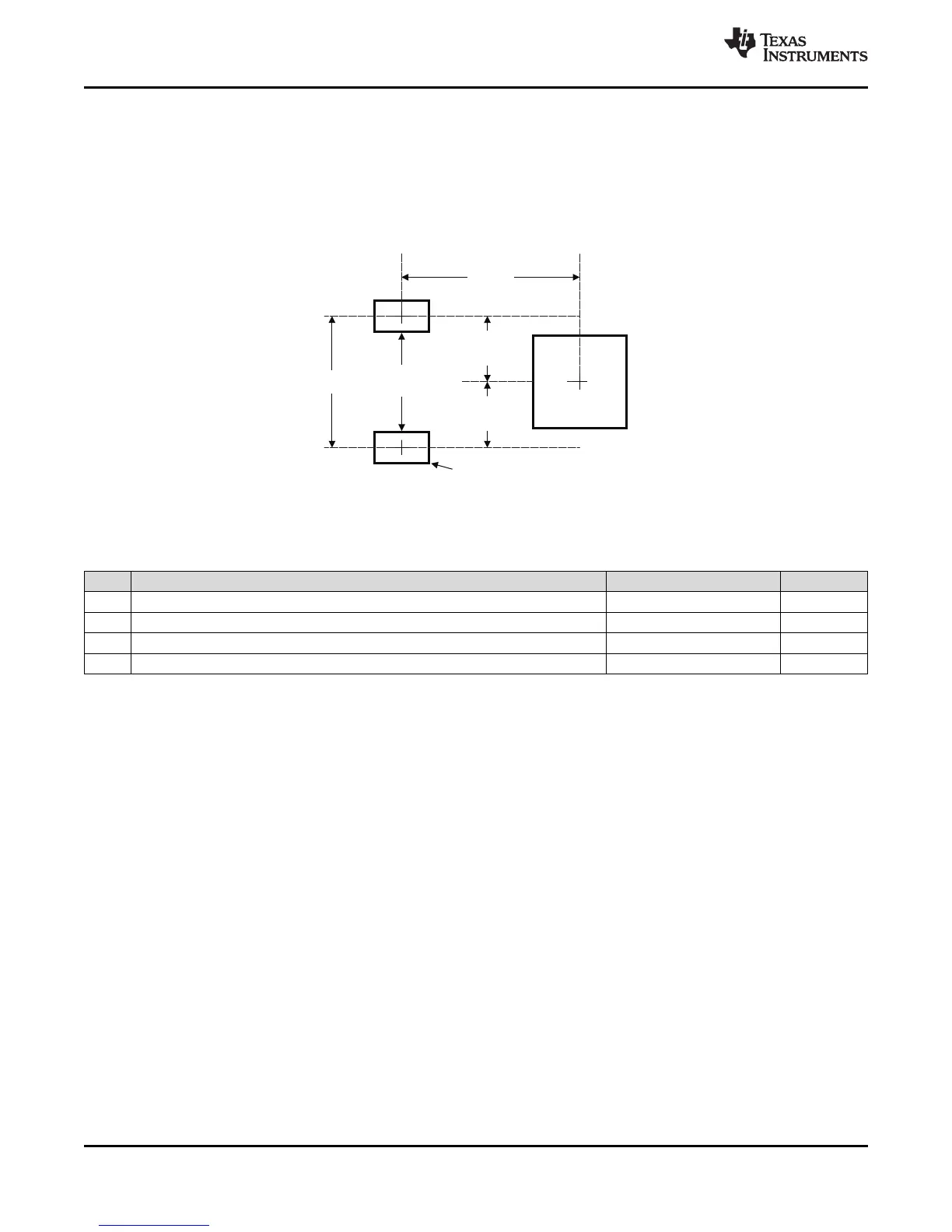
6.11.3.4 Placement
Figure 6-19 shows the required placement for the device as well as the DDR2/mDDR devices. The
dimensions for Figure 6-20 are defined in Table 6-28. The placement does not restrict the side of the PCB
that the devices are mounted on. The ultimate purpose of the placement is to limit the maximum trace
lengths and allow for proper routing space. For single-memory DDR2/mDDR systems, the second
DDR2/mDDR device is omitted from the placement.
Figure 6-20. C6748 and DDR2/mDDR Device Placement
Table 6-28. Placement Specifications
(1)(2)
NO. PARAMETER MIN MAX UNIT
1 X 1750 Mils
2 Y 1280 Mils
3 Y Offset
(3)
650 Mils
4 Clearance from non-DDR2/mDDR signal to DDR2/mDDR Keepout Region
(4)
4 w
(5)
 Loading...


