A1
A1
DDR2/mDDR
Controller
DDR2/mDDR
Device
RegionshouldencompassallDDR2/mDDRcircuitryandvaries
dependingonplacement.Non-DDR2/mDDRsignalsshouldnotbe
routedontheDDRsignallayerswithintheDDR2/mDDRkeepout
region.Non-DDR2/mDDRsignalsmayberoutedintheregion
providedtheyareroutedonlayersseparatedfromDDR2/mDDR
signallayersbyagroundlayer.Nobreaksshouldbeallowedinthe
referencegroundlayersinthisregion.Inaddition,the1.8Vpower
planeshouldcovertheentirekeepoutregion.
125
TMS320C6748
www.ti.com
SPRS590G –JUNE 2009–REVISED JANUARY 2017
Submit Documentation Feedback
Product Folder Links: TMS320C6748
Peripheral Information and Electrical SpecificationsCopyright © 2009–2017, Texas Instruments Incorporated
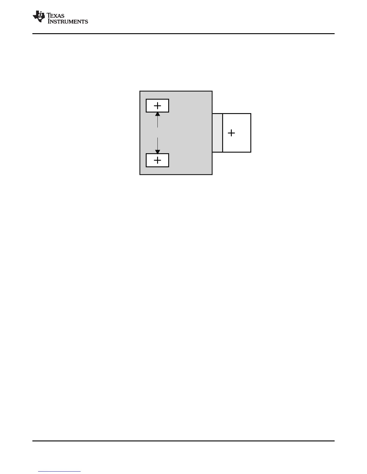
6.11.3.5 DDR2/mDDR Keep Out Region
The region of the PCB used for the DDR2/mDDR circuitry must be isolated from other signals. The
DDR2/mDDR keep out region is defined for this purpose and is shown in Figure 6-21. The size of this
region varies with the placement and DDR routing. Additional clearances required for the keep out region
are shown in Table 6-28.
Figure 6-21. DDR2/mDDR Keepout Region
 Loading...


