A1
A1
T
T
DDR2/mDDR
Controller
F
131
TMS320C6748
www.ti.com
SPRS590G –JUNE 2009–REVISED JANUARY 2017
Submit Documentation Feedback
Product Folder Links: TMS320C6748
Peripheral Information and Electrical SpecificationsCopyright © 2009–2017, Texas Instruments Incorporated
(1) CKB0B1 is the sum of the length of the CK net plus the average length of the DQS0 and DQS1 nets.
(2) w = PCB trace width as defined in Table 6-27.
(3) Skew from CKB0B1
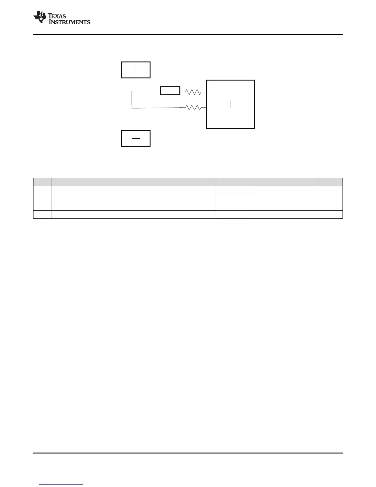
Figure 6-25 shows the routing for the DQGATE net class. Table 6-36 contains the routing specification.
Figure 6-25. DQGATE Routing
Table 6-36. DQGATE Routing Specification
NO. PARAMETER MIN TYP MAX UNIT
1 DQGATE Length F CKB0B
(1)
2 Center to center DQGATE to any other trace spacing 4w
(2)
3 DQS/D nominal trace length DQLM-50 DQLM DQLM+50 Mils
4 DQGATE Skew
(3)
100 Mils
6.11.3.12 DDR2/mDDR Boundary Scan Limitations
Due to DDR implementation and timing restrictions, it was not possible to place boundary scan cells
between core logic and the IO like boundary scan cells for other IO. Instead, the boundary scan cells are
tapped-off to the DDR PHY and there is the equivalent of a multiplexer inside the DDR PHY which selects
between functional and boundary scan paths.
The implication for boundary scan is that the DDR pins will not support the SAMPLE function of the output
enable cells on the DDR pins and this is a violation of IEEE 1149.1. Full EXTEST and PRELOAD
capability is still available.
 Loading...


