A1
A1
E0
T
E1
DDR2/mDDR
Controller
T
130
TMS320C6748
SPRS590G –JUNE 2009–REVISED JANUARY 2017
www.ti.com
Submit Documentation Feedback
Product Folder Links: TMS320C6748
Peripheral Information and Electrical Specifications Copyright © 2009–2017, Texas Instruments Incorporated
(1) Center to center spacing is allowed to fall to minimum (w) for up to 500 mils of routed length to accommodate BGA escape and routing
congestion.
(2) w = PCB trace width as defined in Table 6-27.
(3) Series terminator, if used, should be located closest to DDR.
(4) There is no need and it is not recommended to skew match across data bytes, i.e., from DQS0 and data byte 0 to DQS1 and data byte
1.
(5) D's from other DQS domains are considered other DDR2/mDDR trace.
(6) DQLM is the longest Manhattan distance of each of the DQS and D net class.
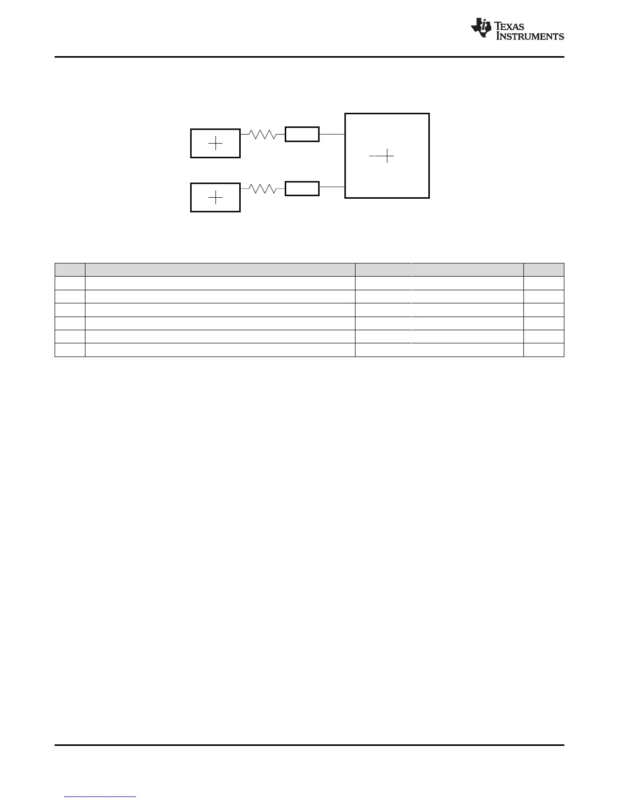
Figure 6-24 shows the topology and routing for the DQS and D net class; the routes are point to point.
Skew matching across bytes is not needed nor recommended.
Figure 6-24. DQS and D Routing and Topology
Table 6-35. DQS and D Routing Specification
NO. PARAMETER MIN TYP MAX UNIT
1 Center to center DQS to other DDR2/mDDR trace spacing
(1)
4w
(2)
2 DQS/D nominal trace length
(3)(4)
DQLM-50 DQLM DQLM+50 Mils
3 D to DQS Skew Length Mismatch
(4)
100 Mils
4 D to D Skew Length Mismatch
(4)
100 Mils
5 Center to center D to other DDR2/mDDR trace spacing
(1)(5)
4w
(2)
6 Center to Center D to other D trace spacing
(1)(6)
3w
(2)
 Loading...


