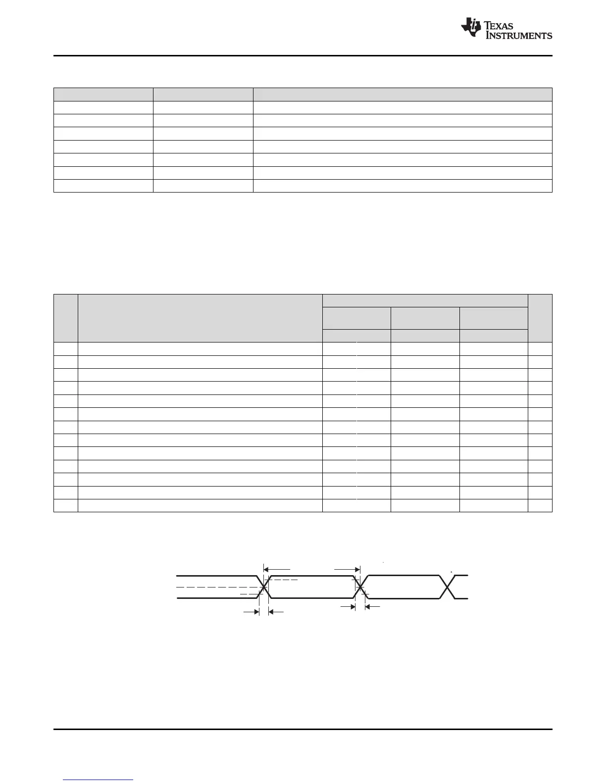
t
r
t
f
V
CRS
90% V
OH
10% V
OL
USB_DM
USB_DP
t
per
−
t
jr
194
TMS320C6748
SPRS590G –JUNE 2009–REVISED JANUARY 2017
www.ti.com
Submit Documentation Feedback
Product Folder Links: TMS320C6748
Peripheral Information and Electrical Specifications Copyright © 2009–2017, Texas Instruments Incorporated
Table 6-90. Universal Serial Bus OTG (USB0) Registers (continued)
BYTE ADDRESS ACRONYM REGISTER DESCRIPTION
0x01E0 6810 QSTATA[1] Queue Manager Queue 1 Status Register A
0x01E0 6814 QSTATB[1] Queue Manager Queue 1 Status Register B
0x01E0 6818 QSTATC[1] Queue Manager Queue 1 Status Register C
. . . . . . . . .
0x01E0 6BF0 QSTATA[63] Queue Manager Queue 63 Status Register A
0x01E0 6BF4 QSTATB[63] Queue Manager Queue 63 Status Register B
0x01E0 6BF8 QSTATC[63] Queue Manager Queue 63 Status Register C
(1) Low Speed: C
L
= 200 pF, Full Speed: C
L
= 50 pF, High Speed: C
L
= 50 pF
(2) t
RFM
= (t
r
/t
f
) x 100. [Excluding the first transaction from the Idle state.]
(3) For more detailed information, see the Universal Serial Bus Specification Revision 2.0, Chapter 7. Electrical.
(4) t
jr
= t
px(1)
- t
px(0)
6.20.1 USB0 [USB2.0] Electrical Data/Timing
The USB PHY PLL can support input clock of the following frequencies: 12.0 MHz, 13.0 MHz, 19.2 MHz,
20.0 MHz, 24.0 MHz, 26.0 MHz, 38.4 MHz, 40.0 MHz or 48.0 MHz. USB_REFCLKIN jitter tolerance is 50
ppm (maximum).
Table 6-91. Switching Characteristics Over Recommended Operating Conditions for USB0 [USB2.0] (see
Figure 6-46)
NO. PARAMETER
1.3V, 1.2V, 1.1V, 1.0V
UNIT
LOW SPEED
1.5 Mbps
FULL SPEED
12 Mbps
HIGH SPEED
480 Mbps
MIN MAX MIN MAX MIN MAX
1 t
r(D)
Rise time, USB_DP and USB_DM signals
(1)
75 300 4 20 0.5 ns
2 t
f(D)
Fall time, USB_DP and USB_DM signals
(1)
75 300 4 20 0.5 ns
3 t
rfM
Rise/Fall time, matching
(2)
80 120 90 111 – – %
4 V
CRS
Output signal cross-over voltage
(1)
1.3 2 1.3 2 – – V
5 t
jr(source)NT
Source (Host) Driver jitter, next transition 2 2
(3)
ns
t
jr(FUNC)NT
Function Driver jitter, next transition 25 2
(3)
ns
6 t
jr(source)PT
Source (Host) Driver jitter, paired transition
(4)
1 1
(3)
ns
t
jr(FUNC)PT
Function Driver jitter, paired transition 10 1
(3)
ns
7 t
w(EOPT)
Pulse duration, EOP transmitter 1250 1500 160 175 – – ns
8 t
w(EOPR)
Pulse duration, EOP receiver 670 82 – ns
9 t
(DRATE)
Data Rate 1.5 12 480 Mb/s
10 Z
DRV
Driver Output Resistance – – 40.5 49.5 40.5 49.5 Ω
11 Z
INP
Receiver Input Impedance 100k 100k - - Ω
Figure 6-46. USB2.0 Integrated Transceiver Interface Timing
 Loading...


