33
TMS320C6748
www.ti.com
SPRS590G –JUNE 2009–REVISED JANUARY 2017
Submit Documentation Feedback
Product Folder Links: TMS320C6748
Device ComparisonCopyright © 2009–2017, Texas Instruments Incorporated
(1) I = Input, O = Output, I/O = Bidirectional, Z = High impedance, PWR = Supply voltage, GND = Ground, A = Analog signal.
Note: The pin type shown refers to the input, output or high-impedance state of the pin function when configured as the signal name
highlighted in bold. All multiplexed signals may enter a high-impedance state when the configured function is input-only or the configured
function supports high-Z operation. All GPIO signals can be used as input or output. For multiplexed pins where functions have different
types (ie., input versus output), the table reflects the pin function direction for that particular peripheral.
(2) IPD = Internal Pulldown resistor; IPU = Internal Pullup resistor; CP[n] = configurable pull-up/pull-down (where n is the pin group) using
the PUPDENA and PUPDSEL registers in the System Module. For more detailed information on pullup/pulldown resistors and situations
where external pullup/pulldown resistors are required, see the Device Configuration section. For electrical specifications on pullup and
internal pulldown circuits, see the Device Operating Conditions section.
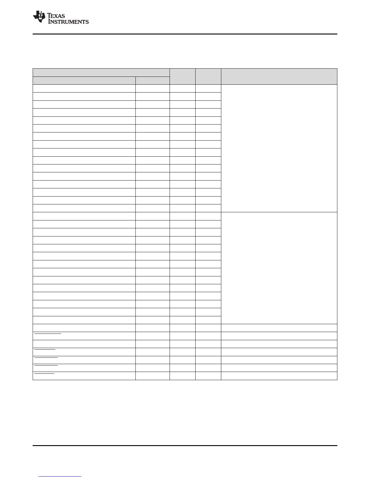
3.7.6 DDR2/mDDR Controller
Table 3-10. DDR2/mDDR Terminal Functions
SIGNAL
TYPE
(1)
PULL
(2)
DESCRIPTION
NAME NO.
DDR_D[15] W10 I/O IPD
DDR2 SDRAM data bus
DDR_D[14] U11 I/O IPD
DDR_D[13] V10 I/O IPD
DDR_D[12] U10 I/O IPD
DDR_D[11] T12 I/O IPD
DDR_D[10] T10 I/O IPD
DDR_D[9] T11 I/O IPD
DDR_D[8] T13 I/O IPD
DDR_D[7] W11 I/O IPD
DDR_D[6] W12 I/O IPD
DDR_D[5] V12 I/O IPD
DDR_D[4] V13 I/O IPD
DDR_D[3] U13 I/O IPD
DDR_D[2] V14 I/O IPD
DDR_D[1] U14 I/O IPD
DDR_D[0] U15 I/O IPD
DDR_A[13] T5 O IPD
DDR2 row/column address
DDR_A[12] V4 O IPD
DDR_A[11] T4 O IPD
DDR_A[10] W4 O IPD
DDR_A[9] T6 O IPD
DDR_A[8] U4 O IPD
DDR_A[7] U6 O IPD
DDR_A[6] W5 O IPD
DDR_A[5] V5 O IPD
DDR_A[4] U5 O IPD
DDR_A[3] V6 O IPD
DDR_A[2] W6 O IPD
DDR_A[1] T7 O IPD
DDR_A[0] U7 O IPD
DDR_CLKP W8 O IPD DDR2 clock (positive)
DDR_CLKN W7 O IPD DDR2 clock (negative)
DDR_CKE V7 O IPD DDR2 clock enable
DDR_WE T8 O IPD DDR2 write enable
DDR_RAS W9 O IPD DDR2 row address strobe
DDR_CAS U9 O IPD DDR2 column address strobe
DDR_CS V9 O IPD DDR2 chip select