54
TMS320C6748
SPRS590G –JUNE 2009–REVISED JANUARY 2017
www.ti.com
Submit Documentation Feedback
Product Folder Links: TMS320C6748
Device Comparison Copyright © 2009–2017, Texas Instruments Incorporated
(1) I = Input, O = Output, I/O = Bidirectional, Z = High impedance, PWR = Supply voltage, GND = Ground, A = Analog signal.
Note: The pin type shown refers to the input, output or high-impedance state of the pin function when configured as the signal name
highlighted in bold. All multiplexed signals may enter a high-impedance state when the configured function is input-only or the configured
function supports high-Z operation. All GPIO signals can be used as input or output. For multiplexed pins where functions have different
types (ie., input versus output), the table reflects the pin function direction for that particular peripheral.
(2) IPD = Internal Pulldown resistor; IPU = Internal Pullup resistor; CP[n] = configurable pull-up/pull-down (where n is the pin group) using
the PUPDENA and PUPDSEL registers in the System Module. The pull-up and pull-down control of these pins is not active until the
device is out of reset. During reset, all of the pins associated with these registers are pulled down. If the application requires a pull-up,
an external pull-up can be used. For more detailed information on pullup/pulldown resistors and situations where external
pullup/pulldown resistors are required, see the Device Configuration section. For electrical specifications on pullup and internal pulldown
circuits, see the Device Operating Conditions section.
(3) This signal is part of a dual-voltage IO group (A, B or C). These groups can be operated at 3.3V or 1.8V nominal. The three groups can
be operated at independent voltages but all pins withina group will operate at the same voltage. Group A operates at the voltage of
power supply DVDD3318_A. Group B operates at the voltage of power supply DVDD3318_B. Group C operates at the voltage of power
supply DVDD3318_C.
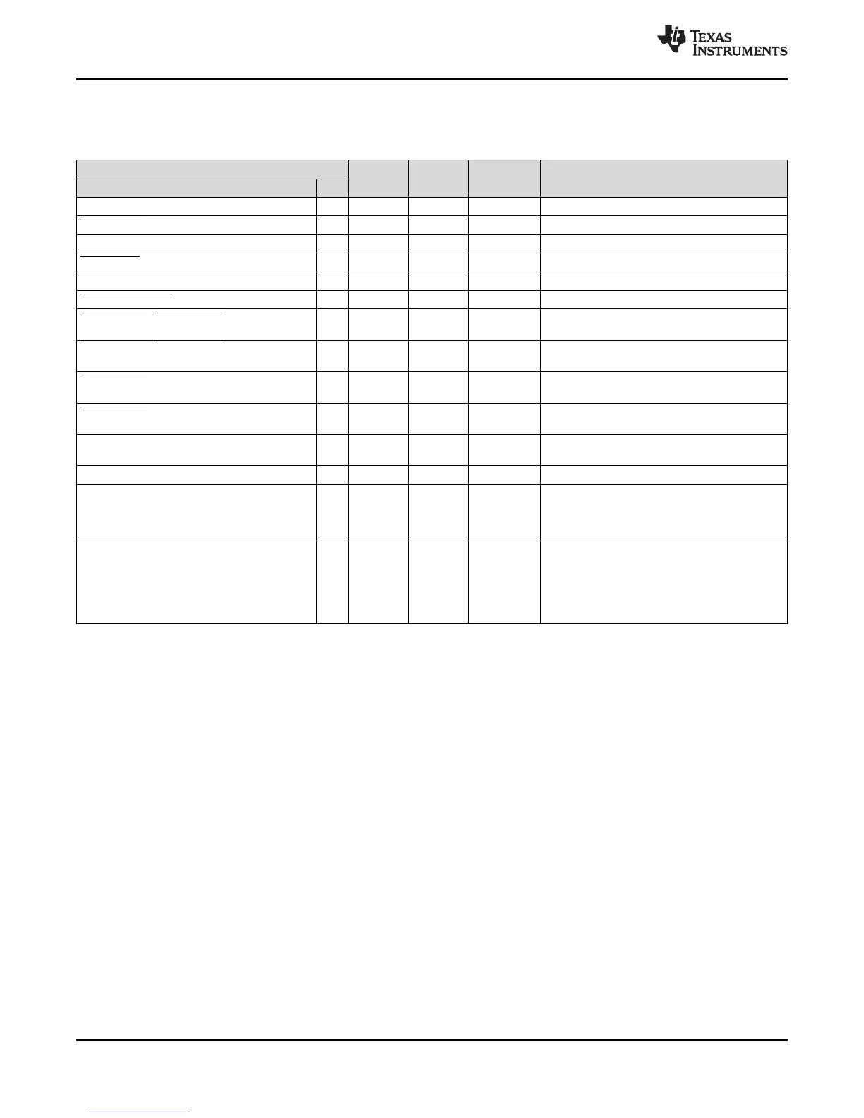
3.7.21 Serial ATA Controller (SATA)
Table 3-25. Serial ATA Controller (SATA) Terminal Functions
SIGNAL
TYPE
(1)
PULL
(2)
POWER
GROUP
(3)
DESCRIPTION
NAME NO.
SATA_RXP L1 I — — SATA receive data (positive)
SATA_RXN L2 I — — SATA receive data (negative)
SATA_TXP J1 O — — SATA transmit data (positive)
SATA_TXN J2 O — — SATA transmit data (negative)
SATA_REFCLKP N2 I — — SATA PHY reference clock (positive)
SATA_REFCLKN N1 I — — SATA PHY reference clock (negative)
SPI0_SCS[3] / UART0_CTS / GP8[2] /
MII_RXD[1] / SATA_MP_SWITCH
E17 I CP[9] A SATA mechanical presence switch input
SPI0_SCS[2] / UART0_RTS / GP8[1] /
MII_RXD[0] / SATA_CP_DET
D16 I CP[9] A SATA cold presence detect input
SPI1_SCS[2] / UART1_TXD /
SATA_CP_POD / GP1[0]
F19 O CP[13] A SATA cold presence power-on output
SPI1_SCS[3] / UART1_RXD / SATA_LED /
GP1[1]
E18 O CP[13] A SATA LED control output
SATA_REG N3 A — —
SATA PHY PLL regulator output. Requires an
external 0.1uF filter capacitor.
SATA_VDDR P3 PWR — — SATA PHY 1.8V internal regulator supply
SATA_VDD
M2,
P1,
P2,
N4
PWR — — SATA PHY 1.2V logic supply
SATA_VSS
H1,
H2,
K1,
K2,
L3,
M1
GND — — SATA PHY ground reference